

Key Insights
The global market for Semiconductor Protective Films is poised for significant expansion, projected to reach $4.1 billion by 2025. This growth is fueled by an impressive Compound Annual Growth Rate (CAGR) of 8.6% anticipated from 2025 to 2033. The increasing complexity and miniaturization of semiconductor devices necessitate advanced protective solutions to ensure their integrity and performance throughout manufacturing and handling processes. Key drivers for this market include the escalating demand for high-performance integrated circuits in consumer electronics, automotive systems, and advanced computing. Furthermore, the burgeoning adoption of 5G technology, artificial intelligence, and the Internet of Things (IoT) are creating a robust pipeline of semiconductor innovation, thereby augmenting the need for specialized protective films. Emerging trends such as the development of thinner, more flexible films with enhanced adhesion properties, and films offering improved electrostatic discharge (ESD) protection are shaping the market landscape. Companies are heavily investing in research and development to cater to these evolving requirements.
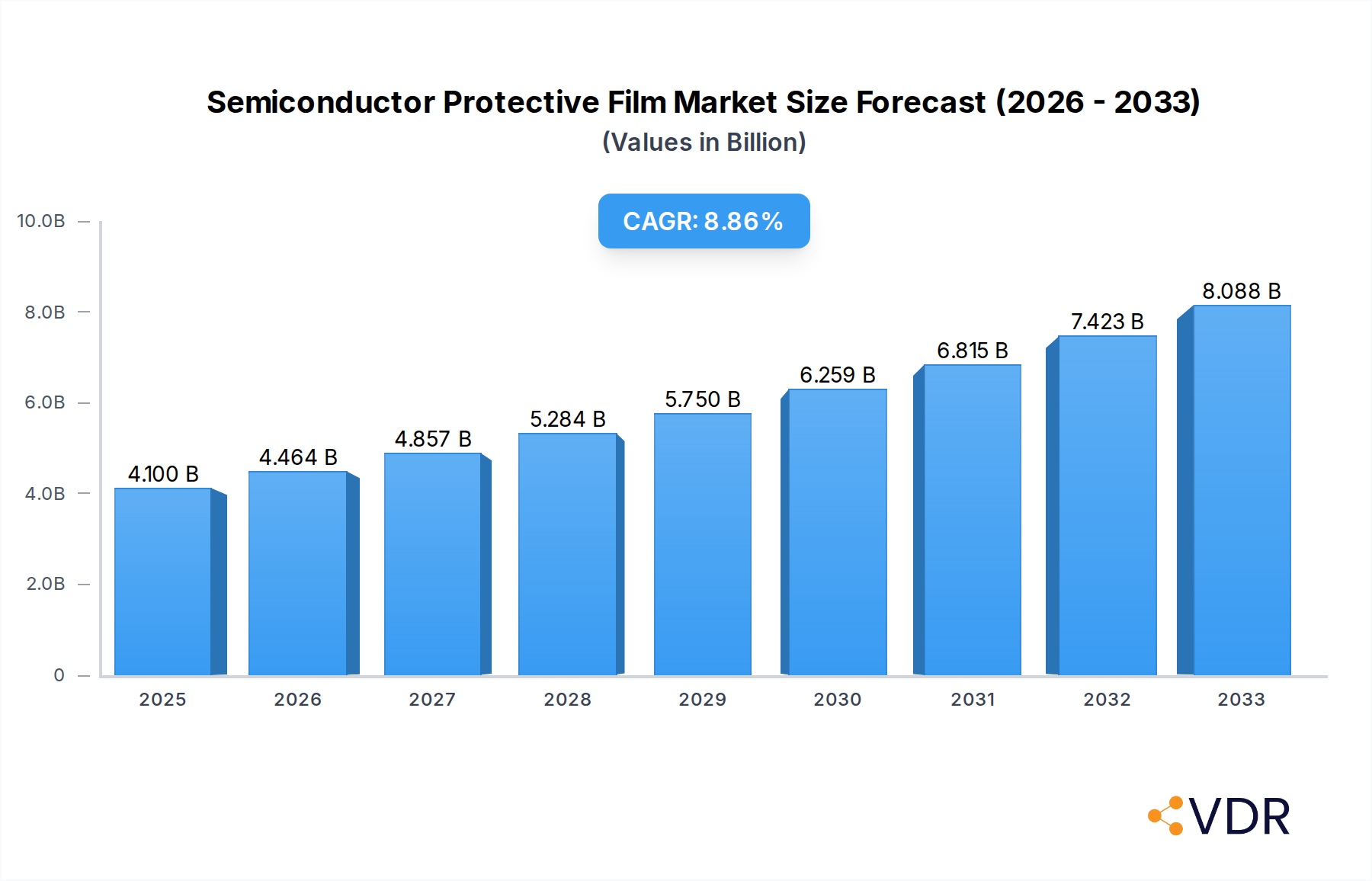
Semiconductor Protective Film Market Size (In Billion)
The market is segmented by application into Front-end Process and Back-end Process, with the latter likely to command a larger share due to the critical need for protection during dicing, packaging, and testing. By type, films are categorized by thickness: Below 100 µm and Above 100 µm. The demand for thinner films is expected to grow as semiconductor devices become more sophisticated and space constraints become paramount. While the market demonstrates strong growth potential, certain restraints, such as the fluctuating raw material costs and the stringent quality control requirements for semiconductor-grade materials, could pose challenges. However, the overall outlook remains highly optimistic, with substantial opportunities anticipated across various geographical regions. Asia Pacific, particularly China and South Korea, is expected to lead in both production and consumption due to its dominance in semiconductor manufacturing.

Semiconductor Protective Film Company Market Share
Semiconductor Protective Film Market: Comprehensive Analysis and Future Outlook (2019-2033)
This in-depth report provides a comprehensive analysis of the global Semiconductor Protective Film market, offering critical insights into its dynamics, growth trajectory, and future potential. Covering the historical period from 2019 to 2024, with a base and estimated year of 2025, and a robust forecast period extending to 2033, this report is an indispensable resource for industry stakeholders seeking to navigate the evolving landscape of semiconductor manufacturing.
Semiconductor Protective Film Market Dynamics & Structure
The global Semiconductor Protective Film market is characterized by a moderately consolidated structure, with key players like Mitsui Chemicals and Nitto Denko holding significant market share. Technological innovation is the primary driver, fueled by the relentless pursuit of smaller, more powerful, and reliable semiconductor devices. Advancements in material science, particularly in developing films with enhanced adhesion, thermal resistance, and optical clarity, are crucial. Regulatory frameworks, while generally supportive of the semiconductor industry's growth, can indirectly influence the market through environmental compliance and material safety standards. Competitive product substitutes, though limited in direct overlap, include alternative masking or packaging solutions that could emerge with significant technological breakthroughs.
- Market Concentration: Dominated by a few key global manufacturers, with a growing presence of regional players in Asia-Pacific.
- Technological Innovation Drivers: Miniaturization of semiconductors, increased wafer complexity, and demand for higher yields necessitate advanced protective films.
- Regulatory Frameworks: Focus on material safety, environmental impact, and industry-specific standards.
- Competitive Product Substitutes: Emerging advanced masking techniques or innovative packaging materials could pose indirect competition.
- End-User Demographics: Primarily semiconductor fabrication plants (fabs), outsourced semiconductor assembly and test (OSAT) facilities, and equipment manufacturers.
- M&A Trends: Expect strategic acquisitions by larger players to gain access to new technologies or expand geographical reach. For instance, the market has witnessed an estimated xx M&A deals in the historical period (2019-2024).
Semiconductor Protective Film Growth Trends & Insights
The Semiconductor Protective Film market is projected for substantial growth, driven by the ever-increasing demand for semiconductors across various end-use industries. The market size is anticipated to grow from an estimated \$xx billion in the base year 2025 to \$xx billion by 2033, exhibiting a Compound Annual Growth Rate (CAGR) of xx% during the forecast period (2025–2033). This impressive growth trajectory is underpinned by the relentless pace of technological advancements in the semiconductor industry, including the transition to advanced nodes (e.g., 3nm, 2nm) and the increasing complexity of wafer fabrication processes.
The adoption rate of advanced semiconductor protective films is soaring as manufacturers recognize their critical role in enhancing wafer yield, reducing defect rates, and protecting sensitive circuitry during intricate manufacturing stages. Disruptive technologies like Extreme Ultraviolet (EUV) lithography and advanced packaging techniques are not only creating new demands for specialized protective films but also driving innovation in material properties such as ultra-low particle generation and superior chemical resistance. Consumer behavior shifts towards devices with higher performance, greater connectivity, and extended battery life are indirectly fueling the demand for more sophisticated semiconductor components, thereby boosting the need for high-performance protective films.
The parent market for Semiconductor Protective Film is the broader Semiconductor Manufacturing Materials market, which was valued at approximately \$xx billion in 2025. Within this, the child market of Semiconductor Protective Film is a rapidly expanding segment. Key insights into growth include:
- Market Size Evolution: The market is projected to expand significantly, driven by increased semiconductor production volumes and the need for higher-quality protective solutions.
- Adoption Rates: High adoption rates are expected for films catering to advanced fabrication processes and new material compositions.
- Technological Disruptions: Innovations in lithography, etching, and polishing technologies directly influence the requirements for protective films.
- Consumer Behavior Shifts: Growing demand for AI-powered devices, 5G connectivity, and IoT solutions translates to increased semiconductor demand, benefiting the protective film market.
- Market Penetration: Expected to increase as new applications and stricter quality control measures become standard in semiconductor manufacturing.
- CAGR: The market is poised for a robust CAGR of xx% from 2025 to 2033, indicating strong and sustained growth.
Dominant Regions, Countries, or Segments in Semiconductor Protective Film
The Application segment of Front-end Process is currently the dominant driver of growth within the global Semiconductor Protective Film market. This segment encompasses the critical stages of wafer fabrication, where protective films are essential for masking, handling, and protecting delicate wafer surfaces during lithography, etching, deposition, and cleaning processes. The increasing complexity of advanced semiconductor nodes, such as those below 10nm, necessitates highly specialized and precise protective films to ensure minimal defects and high yields. The rising investment in new fab constructions and the expansion of existing facilities, particularly in Asia-Pacific, further bolsters the demand for front-end process films.
- Dominant Segment (Application): Front-end Process. This segment accounts for an estimated xx% of the total Semiconductor Protective Film market in 2025, with a projected growth rate of xx% during the forecast period.
- Key Drivers for Front-end Process Dominance:
- Advanced Node Manufacturing: The push towards 3nm, 2nm, and beyond requires ultra-thin, high-purity films for photolithography and etching.
- EUV Lithography: This technology demands highly specialized films for reticle protection and wafer handling.
- Increased Wafer Complexity: Multi-layer structures and intricate designs necessitate robust protection during fabrication.
- High Yield Requirements: The cost of defects in the front-end process is substantial, driving the demand for premium protective films.
- Leading Region: Asia-Pacific, driven by its status as the global semiconductor manufacturing hub, particularly Taiwan, South Korea, and China. This region is estimated to hold a xx% market share in 2025.
- Dominant Country: Taiwan, with its extensive concentration of leading foundries.
- Dominant Type: Thickness Below 100㎛ films are crucial for the intricate front-end processes, accounting for approximately xx% of the market in 2025.
- Growth Potential: The Back-end Process segment is also witnessing significant growth due to advanced packaging technologies, presenting a strong secondary growth avenue.
Semiconductor Protective Film Product Landscape
The Semiconductor Protective Film market is witnessing a surge in product innovation focused on enhancing performance and addressing the evolving needs of semiconductor manufacturing. Companies are developing ultra-thin films (below 100 µm) with superior adhesion properties for precise masking and protection during lithography, as well as robust, thicker films (above 100 µm) designed for enhanced handling and protection during wafer dicing and packaging. Key advancements include the development of films with reduced particle generation, improved chemical resistance for aggressive processing environments, and enhanced optical clarity for metrology applications. These innovations are critical for improving manufacturing yields, reducing defect rates, and enabling the production of next-generation semiconductor devices.
Key Drivers, Barriers & Challenges in Semiconductor Protective Film
Key Drivers:
- Exponential Growth in Semiconductor Demand: Driven by AI, 5G, IoT, and advanced computing, leading to increased fab capacity and protective film consumption.
- Technological Advancements in Chip Manufacturing: The continuous pursuit of smaller process nodes and complex architectures necessitates higher-performance protective films.
- Focus on Yield Improvement and Defect Reduction: Protective films play a crucial role in minimizing contamination and damage, directly impacting manufacturing yields.
- Emergence of New Packaging Technologies: Advanced packaging solutions require specialized protective films for enhanced reliability and performance.
Barriers & Challenges:
- High Cost of R&D and Manufacturing: Developing and producing specialized semiconductor protective films requires significant investment.
- Stringent Quality and Purity Requirements: Even trace contaminants can be detrimental, leading to rigorous quality control demands.
- Supply Chain Volatility: Global supply chain disruptions can impact the availability of raw materials and the timely delivery of finished products, a challenge estimated to affect xx% of manufacturers in the past.
- Intense Competition and Price Pressure: While specialization is key, a competitive landscape can lead to price pressures, impacting profit margins.
- Technological Obsolescence: Rapid advancements in semiconductor technology can quickly render existing protective film solutions outdated.
Emerging Opportunities in Semiconductor Protective Film
The Semiconductor Protective Film market is ripe with emerging opportunities. The growing demand for specialized films in emerging applications such as flexible electronics, advanced sensors, and compound semiconductors presents significant untapped potential. Furthermore, the increasing adoption of sustainable manufacturing practices is driving demand for eco-friendly and recyclable protective film materials. Innovations in smart films with integrated sensing capabilities for real-time process monitoring also represent a promising area for future growth and differentiation.
Growth Accelerators in the Semiconductor Protective Film Industry
Several factors are accelerating the long-term growth of the Semiconductor Protective Film industry. These include the ongoing global investment in semiconductor manufacturing capacity, spurred by geopolitical considerations and the desire for supply chain resilience. Strategic partnerships between protective film manufacturers and leading semiconductor equipment and material providers are fostering innovation and accelerating product development. The increasing standardization of certain protective film types for high-volume manufacturing processes is also contributing to market expansion. Furthermore, the development of novel materials with enhanced properties, such as superior thermal management capabilities or self-healing functionalities, will act as significant growth catalysts.
Key Players Shaping the Semiconductor Protective Film Market
- Mitsui Chemicals
- Nitto Denko
- AMC
- Harima Chemicals
- Deep Materials
- Shanghai Lanqing
- Hengchuang Material
- Koatech
- Tsinghon
Notable Milestones in Semiconductor Protective Film Sector
- 2019: Increased focus on thinner films for advanced EUV lithography applications.
- 2020: Major players announce R&D investments in biodegradable protective films to meet sustainability demands.
- 2021: Launch of novel protective films with enhanced particle-free properties for sensitive wafer processes.
- 2022: Significant M&A activity as larger chemical companies acquire specialized protective film manufacturers to expand their semiconductor materials portfolio.
- 2023: Introduction of protective films with improved chemical resistance for advanced etching and cleaning chemistries.
- 2024: Growing demand for customized protective film solutions tailored to specific semiconductor device architectures.
In-Depth Semiconductor Protective Film Market Outlook
The future outlook for the Semiconductor Protective Film market is exceptionally bright, fueled by an unwavering demand for semiconductors and the relentless march of technological innovation. Growth accelerators, including massive global investments in semiconductor manufacturing capacity and strategic collaborations between key industry players, will ensure sustained expansion. The development of next-generation materials with superior functionalities, coupled with the exploration of new application frontiers in emerging technologies, will further bolster market potential. Companies that prioritize continuous innovation, adapt to evolving regulatory landscapes, and strategically address supply chain challenges will be well-positioned to capitalize on the significant opportunities within this dynamic sector.
Semiconductor Protective Film Segmentation
-
1. Application
- 1.1. Front-end Process
- 1.2. Back-end Process
-
2. Types
- 2.1. Thickness Below 100㎛
- 2.2. Thickness Above 100㎛
Semiconductor Protective Film Segmentation By Geography
-
1. North America
- 1.1. United States
- 1.2. Canada
- 1.3. Mexico
-
2. South America
- 2.1. Brazil
- 2.2. Argentina
- 2.3. Rest of South America
-
3. Europe
- 3.1. United Kingdom
- 3.2. Germany
- 3.3. France
- 3.4. Italy
- 3.5. Spain
- 3.6. Russia
- 3.7. Benelux
- 3.8. Nordics
- 3.9. Rest of Europe
-
4. Middle East & Africa
- 4.1. Turkey
- 4.2. Israel
- 4.3. GCC
- 4.4. North Africa
- 4.5. South Africa
- 4.6. Rest of Middle East & Africa
-
5. Asia Pacific
- 5.1. China
- 5.2. India
- 5.3. Japan
- 5.4. South Korea
- 5.5. ASEAN
- 5.6. Oceania
- 5.7. Rest of Asia Pacific
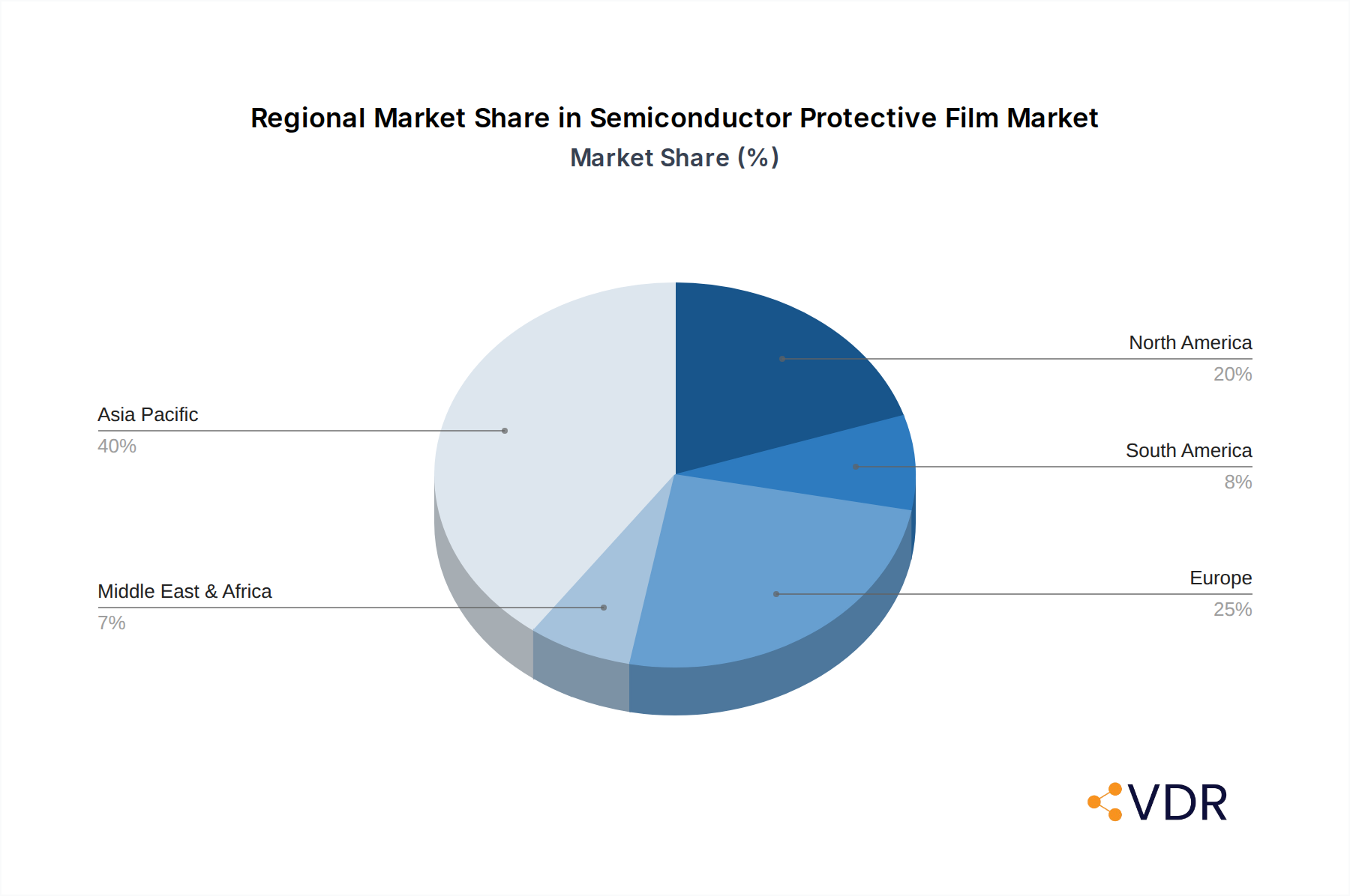
Semiconductor Protective Film Regional Market Share
Geographic Coverage of Semiconductor Protective Film
Semiconductor Protective Film REPORT HIGHLIGHTS
| Aspects | Details |
|---|---|
| Study Period | 2020-2034 |
| Base Year | 2025 |
| Estimated Year | 2026 |
| Forecast Period | 2026-2034 |
| Historical Period | 2020-2025 |
| Growth Rate | CAGR of 8.6% from 2020-2034 |
| Segmentation |
|
Table of Contents
- 1. Introduction
- 1.1. Research Scope
- 1.2. Market Segmentation
- 1.3. Research Methodology
- 1.4. Definitions and Assumptions
- 2. Executive Summary
- 2.1. Introduction
- 3. Market Dynamics
- 3.1. Introduction
- 3.2. Market Drivers
- 3.3. Market Restrains
- 3.4. Market Trends
- 4. Market Factor Analysis
- 4.1. Porters Five Forces
- 4.2. Supply/Value Chain
- 4.3. PESTEL analysis
- 4.4. Market Entropy
- 4.5. Patent/Trademark Analysis
- 5. Global Semiconductor Protective Film Analysis, Insights and Forecast, 2020-2032
- 5.1. Market Analysis, Insights and Forecast - by Application
- 5.1.1. Front-end Process
- 5.1.2. Back-end Process
- 5.2. Market Analysis, Insights and Forecast - by Types
- 5.2.1. Thickness Below 100㎛
- 5.2.2. Thickness Above 100㎛
- 5.3. Market Analysis, Insights and Forecast - by Region
- 5.3.1. North America
- 5.3.2. South America
- 5.3.3. Europe
- 5.3.4. Middle East & Africa
- 5.3.5. Asia Pacific
- 5.1. Market Analysis, Insights and Forecast - by Application
- 6. North America Semiconductor Protective Film Analysis, Insights and Forecast, 2020-2032
- 6.1. Market Analysis, Insights and Forecast - by Application
- 6.1.1. Front-end Process
- 6.1.2. Back-end Process
- 6.2. Market Analysis, Insights and Forecast - by Types
- 6.2.1. Thickness Below 100㎛
- 6.2.2. Thickness Above 100㎛
- 6.1. Market Analysis, Insights and Forecast - by Application
- 7. South America Semiconductor Protective Film Analysis, Insights and Forecast, 2020-2032
- 7.1. Market Analysis, Insights and Forecast - by Application
- 7.1.1. Front-end Process
- 7.1.2. Back-end Process
- 7.2. Market Analysis, Insights and Forecast - by Types
- 7.2.1. Thickness Below 100㎛
- 7.2.2. Thickness Above 100㎛
- 7.1. Market Analysis, Insights and Forecast - by Application
- 8. Europe Semiconductor Protective Film Analysis, Insights and Forecast, 2020-2032
- 8.1. Market Analysis, Insights and Forecast - by Application
- 8.1.1. Front-end Process
- 8.1.2. Back-end Process
- 8.2. Market Analysis, Insights and Forecast - by Types
- 8.2.1. Thickness Below 100㎛
- 8.2.2. Thickness Above 100㎛
- 8.1. Market Analysis, Insights and Forecast - by Application
- 9. Middle East & Africa Semiconductor Protective Film Analysis, Insights and Forecast, 2020-2032
- 9.1. Market Analysis, Insights and Forecast - by Application
- 9.1.1. Front-end Process
- 9.1.2. Back-end Process
- 9.2. Market Analysis, Insights and Forecast - by Types
- 9.2.1. Thickness Below 100㎛
- 9.2.2. Thickness Above 100㎛
- 9.1. Market Analysis, Insights and Forecast - by Application
- 10. Asia Pacific Semiconductor Protective Film Analysis, Insights and Forecast, 2020-2032
- 10.1. Market Analysis, Insights and Forecast - by Application
- 10.1.1. Front-end Process
- 10.1.2. Back-end Process
- 10.2. Market Analysis, Insights and Forecast - by Types
- 10.2.1. Thickness Below 100㎛
- 10.2.2. Thickness Above 100㎛
- 10.1. Market Analysis, Insights and Forecast - by Application
- 11. Competitive Analysis
- 11.1. Global Market Share Analysis 2025
- 11.2. Company Profiles
- 11.2.1 Mitsui Chemicals
- 11.2.1.1. Overview
- 11.2.1.2. Products
- 11.2.1.3. SWOT Analysis
- 11.2.1.4. Recent Developments
- 11.2.1.5. Financials (Based on Availability)
- 11.2.2 Nitto Denko
- 11.2.2.1. Overview
- 11.2.2.2. Products
- 11.2.2.3. SWOT Analysis
- 11.2.2.4. Recent Developments
- 11.2.2.5. Financials (Based on Availability)
- 11.2.3 AMC
- 11.2.3.1. Overview
- 11.2.3.2. Products
- 11.2.3.3. SWOT Analysis
- 11.2.3.4. Recent Developments
- 11.2.3.5. Financials (Based on Availability)
- 11.2.4 Harima Chemicals
- 11.2.4.1. Overview
- 11.2.4.2. Products
- 11.2.4.3. SWOT Analysis
- 11.2.4.4. Recent Developments
- 11.2.4.5. Financials (Based on Availability)
- 11.2.5 Deep Materials
- 11.2.5.1. Overview
- 11.2.5.2. Products
- 11.2.5.3. SWOT Analysis
- 11.2.5.4. Recent Developments
- 11.2.5.5. Financials (Based on Availability)
- 11.2.6 Shanghai Lanqing
- 11.2.6.1. Overview
- 11.2.6.2. Products
- 11.2.6.3. SWOT Analysis
- 11.2.6.4. Recent Developments
- 11.2.6.5. Financials (Based on Availability)
- 11.2.7 Hengchuang Material
- 11.2.7.1. Overview
- 11.2.7.2. Products
- 11.2.7.3. SWOT Analysis
- 11.2.7.4. Recent Developments
- 11.2.7.5. Financials (Based on Availability)
- 11.2.8 Koatech
- 11.2.8.1. Overview
- 11.2.8.2. Products
- 11.2.8.3. SWOT Analysis
- 11.2.8.4. Recent Developments
- 11.2.8.5. Financials (Based on Availability)
- 11.2.9 Tsinghon
- 11.2.9.1. Overview
- 11.2.9.2. Products
- 11.2.9.3. SWOT Analysis
- 11.2.9.4. Recent Developments
- 11.2.9.5. Financials (Based on Availability)
- 11.2.1 Mitsui Chemicals
List of Figures
- Figure 1: Global Semiconductor Protective Film Revenue Breakdown (undefined, %) by Region 2025 & 2033
- Figure 2: Global Semiconductor Protective Film Volume Breakdown (K, %) by Region 2025 & 2033
- Figure 3: North America Semiconductor Protective Film Revenue (undefined), by Application 2025 & 2033
- Figure 4: North America Semiconductor Protective Film Volume (K), by Application 2025 & 2033
- Figure 5: North America Semiconductor Protective Film Revenue Share (%), by Application 2025 & 2033
- Figure 6: North America Semiconductor Protective Film Volume Share (%), by Application 2025 & 2033
- Figure 7: North America Semiconductor Protective Film Revenue (undefined), by Types 2025 & 2033
- Figure 8: North America Semiconductor Protective Film Volume (K), by Types 2025 & 2033
- Figure 9: North America Semiconductor Protective Film Revenue Share (%), by Types 2025 & 2033
- Figure 10: North America Semiconductor Protective Film Volume Share (%), by Types 2025 & 2033
- Figure 11: North America Semiconductor Protective Film Revenue (undefined), by Country 2025 & 2033
- Figure 12: North America Semiconductor Protective Film Volume (K), by Country 2025 & 2033
- Figure 13: North America Semiconductor Protective Film Revenue Share (%), by Country 2025 & 2033
- Figure 14: North America Semiconductor Protective Film Volume Share (%), by Country 2025 & 2033
- Figure 15: South America Semiconductor Protective Film Revenue (undefined), by Application 2025 & 2033
- Figure 16: South America Semiconductor Protective Film Volume (K), by Application 2025 & 2033
- Figure 17: South America Semiconductor Protective Film Revenue Share (%), by Application 2025 & 2033
- Figure 18: South America Semiconductor Protective Film Volume Share (%), by Application 2025 & 2033
- Figure 19: South America Semiconductor Protective Film Revenue (undefined), by Types 2025 & 2033
- Figure 20: South America Semiconductor Protective Film Volume (K), by Types 2025 & 2033
- Figure 21: South America Semiconductor Protective Film Revenue Share (%), by Types 2025 & 2033
- Figure 22: South America Semiconductor Protective Film Volume Share (%), by Types 2025 & 2033
- Figure 23: South America Semiconductor Protective Film Revenue (undefined), by Country 2025 & 2033
- Figure 24: South America Semiconductor Protective Film Volume (K), by Country 2025 & 2033
- Figure 25: South America Semiconductor Protective Film Revenue Share (%), by Country 2025 & 2033
- Figure 26: South America Semiconductor Protective Film Volume Share (%), by Country 2025 & 2033
- Figure 27: Europe Semiconductor Protective Film Revenue (undefined), by Application 2025 & 2033
- Figure 28: Europe Semiconductor Protective Film Volume (K), by Application 2025 & 2033
- Figure 29: Europe Semiconductor Protective Film Revenue Share (%), by Application 2025 & 2033
- Figure 30: Europe Semiconductor Protective Film Volume Share (%), by Application 2025 & 2033
- Figure 31: Europe Semiconductor Protective Film Revenue (undefined), by Types 2025 & 2033
- Figure 32: Europe Semiconductor Protective Film Volume (K), by Types 2025 & 2033
- Figure 33: Europe Semiconductor Protective Film Revenue Share (%), by Types 2025 & 2033
- Figure 34: Europe Semiconductor Protective Film Volume Share (%), by Types 2025 & 2033
- Figure 35: Europe Semiconductor Protective Film Revenue (undefined), by Country 2025 & 2033
- Figure 36: Europe Semiconductor Protective Film Volume (K), by Country 2025 & 2033
- Figure 37: Europe Semiconductor Protective Film Revenue Share (%), by Country 2025 & 2033
- Figure 38: Europe Semiconductor Protective Film Volume Share (%), by Country 2025 & 2033
- Figure 39: Middle East & Africa Semiconductor Protective Film Revenue (undefined), by Application 2025 & 2033
- Figure 40: Middle East & Africa Semiconductor Protective Film Volume (K), by Application 2025 & 2033
- Figure 41: Middle East & Africa Semiconductor Protective Film Revenue Share (%), by Application 2025 & 2033
- Figure 42: Middle East & Africa Semiconductor Protective Film Volume Share (%), by Application 2025 & 2033
- Figure 43: Middle East & Africa Semiconductor Protective Film Revenue (undefined), by Types 2025 & 2033
- Figure 44: Middle East & Africa Semiconductor Protective Film Volume (K), by Types 2025 & 2033
- Figure 45: Middle East & Africa Semiconductor Protective Film Revenue Share (%), by Types 2025 & 2033
- Figure 46: Middle East & Africa Semiconductor Protective Film Volume Share (%), by Types 2025 & 2033
- Figure 47: Middle East & Africa Semiconductor Protective Film Revenue (undefined), by Country 2025 & 2033
- Figure 48: Middle East & Africa Semiconductor Protective Film Volume (K), by Country 2025 & 2033
- Figure 49: Middle East & Africa Semiconductor Protective Film Revenue Share (%), by Country 2025 & 2033
- Figure 50: Middle East & Africa Semiconductor Protective Film Volume Share (%), by Country 2025 & 2033
- Figure 51: Asia Pacific Semiconductor Protective Film Revenue (undefined), by Application 2025 & 2033
- Figure 52: Asia Pacific Semiconductor Protective Film Volume (K), by Application 2025 & 2033
- Figure 53: Asia Pacific Semiconductor Protective Film Revenue Share (%), by Application 2025 & 2033
- Figure 54: Asia Pacific Semiconductor Protective Film Volume Share (%), by Application 2025 & 2033
- Figure 55: Asia Pacific Semiconductor Protective Film Revenue (undefined), by Types 2025 & 2033
- Figure 56: Asia Pacific Semiconductor Protective Film Volume (K), by Types 2025 & 2033
- Figure 57: Asia Pacific Semiconductor Protective Film Revenue Share (%), by Types 2025 & 2033
- Figure 58: Asia Pacific Semiconductor Protective Film Volume Share (%), by Types 2025 & 2033
- Figure 59: Asia Pacific Semiconductor Protective Film Revenue (undefined), by Country 2025 & 2033
- Figure 60: Asia Pacific Semiconductor Protective Film Volume (K), by Country 2025 & 2033
- Figure 61: Asia Pacific Semiconductor Protective Film Revenue Share (%), by Country 2025 & 2033
- Figure 62: Asia Pacific Semiconductor Protective Film Volume Share (%), by Country 2025 & 2033
List of Tables
- Table 1: Global Semiconductor Protective Film Revenue undefined Forecast, by Application 2020 & 2033
- Table 2: Global Semiconductor Protective Film Volume K Forecast, by Application 2020 & 2033
- Table 3: Global Semiconductor Protective Film Revenue undefined Forecast, by Types 2020 & 2033
- Table 4: Global Semiconductor Protective Film Volume K Forecast, by Types 2020 & 2033
- Table 5: Global Semiconductor Protective Film Revenue undefined Forecast, by Region 2020 & 2033
- Table 6: Global Semiconductor Protective Film Volume K Forecast, by Region 2020 & 2033
- Table 7: Global Semiconductor Protective Film Revenue undefined Forecast, by Application 2020 & 2033
- Table 8: Global Semiconductor Protective Film Volume K Forecast, by Application 2020 & 2033
- Table 9: Global Semiconductor Protective Film Revenue undefined Forecast, by Types 2020 & 2033
- Table 10: Global Semiconductor Protective Film Volume K Forecast, by Types 2020 & 2033
- Table 11: Global Semiconductor Protective Film Revenue undefined Forecast, by Country 2020 & 2033
- Table 12: Global Semiconductor Protective Film Volume K Forecast, by Country 2020 & 2033
- Table 13: United States Semiconductor Protective Film Revenue (undefined) Forecast, by Application 2020 & 2033
- Table 14: United States Semiconductor Protective Film Volume (K) Forecast, by Application 2020 & 2033
- Table 15: Canada Semiconductor Protective Film Revenue (undefined) Forecast, by Application 2020 & 2033
- Table 16: Canada Semiconductor Protective Film Volume (K) Forecast, by Application 2020 & 2033
- Table 17: Mexico Semiconductor Protective Film Revenue (undefined) Forecast, by Application 2020 & 2033
- Table 18: Mexico Semiconductor Protective Film Volume (K) Forecast, by Application 2020 & 2033
- Table 19: Global Semiconductor Protective Film Revenue undefined Forecast, by Application 2020 & 2033
- Table 20: Global Semiconductor Protective Film Volume K Forecast, by Application 2020 & 2033
- Table 21: Global Semiconductor Protective Film Revenue undefined Forecast, by Types 2020 & 2033
- Table 22: Global Semiconductor Protective Film Volume K Forecast, by Types 2020 & 2033
- Table 23: Global Semiconductor Protective Film Revenue undefined Forecast, by Country 2020 & 2033
- Table 24: Global Semiconductor Protective Film Volume K Forecast, by Country 2020 & 2033
- Table 25: Brazil Semiconductor Protective Film Revenue (undefined) Forecast, by Application 2020 & 2033
- Table 26: Brazil Semiconductor Protective Film Volume (K) Forecast, by Application 2020 & 2033
- Table 27: Argentina Semiconductor Protective Film Revenue (undefined) Forecast, by Application 2020 & 2033
- Table 28: Argentina Semiconductor Protective Film Volume (K) Forecast, by Application 2020 & 2033
- Table 29: Rest of South America Semiconductor Protective Film Revenue (undefined) Forecast, by Application 2020 & 2033
- Table 30: Rest of South America Semiconductor Protective Film Volume (K) Forecast, by Application 2020 & 2033
- Table 31: Global Semiconductor Protective Film Revenue undefined Forecast, by Application 2020 & 2033
- Table 32: Global Semiconductor Protective Film Volume K Forecast, by Application 2020 & 2033
- Table 33: Global Semiconductor Protective Film Revenue undefined Forecast, by Types 2020 & 2033
- Table 34: Global Semiconductor Protective Film Volume K Forecast, by Types 2020 & 2033
- Table 35: Global Semiconductor Protective Film Revenue undefined Forecast, by Country 2020 & 2033
- Table 36: Global Semiconductor Protective Film Volume K Forecast, by Country 2020 & 2033
- Table 37: United Kingdom Semiconductor Protective Film Revenue (undefined) Forecast, by Application 2020 & 2033
- Table 38: United Kingdom Semiconductor Protective Film Volume (K) Forecast, by Application 2020 & 2033
- Table 39: Germany Semiconductor Protective Film Revenue (undefined) Forecast, by Application 2020 & 2033
- Table 40: Germany Semiconductor Protective Film Volume (K) Forecast, by Application 2020 & 2033
- Table 41: France Semiconductor Protective Film Revenue (undefined) Forecast, by Application 2020 & 2033
- Table 42: France Semiconductor Protective Film Volume (K) Forecast, by Application 2020 & 2033
- Table 43: Italy Semiconductor Protective Film Revenue (undefined) Forecast, by Application 2020 & 2033
- Table 44: Italy Semiconductor Protective Film Volume (K) Forecast, by Application 2020 & 2033
- Table 45: Spain Semiconductor Protective Film Revenue (undefined) Forecast, by Application 2020 & 2033
- Table 46: Spain Semiconductor Protective Film Volume (K) Forecast, by Application 2020 & 2033
- Table 47: Russia Semiconductor Protective Film Revenue (undefined) Forecast, by Application 2020 & 2033
- Table 48: Russia Semiconductor Protective Film Volume (K) Forecast, by Application 2020 & 2033
- Table 49: Benelux Semiconductor Protective Film Revenue (undefined) Forecast, by Application 2020 & 2033
- Table 50: Benelux Semiconductor Protective Film Volume (K) Forecast, by Application 2020 & 2033
- Table 51: Nordics Semiconductor Protective Film Revenue (undefined) Forecast, by Application 2020 & 2033
- Table 52: Nordics Semiconductor Protective Film Volume (K) Forecast, by Application 2020 & 2033
- Table 53: Rest of Europe Semiconductor Protective Film Revenue (undefined) Forecast, by Application 2020 & 2033
- Table 54: Rest of Europe Semiconductor Protective Film Volume (K) Forecast, by Application 2020 & 2033
- Table 55: Global Semiconductor Protective Film Revenue undefined Forecast, by Application 2020 & 2033
- Table 56: Global Semiconductor Protective Film Volume K Forecast, by Application 2020 & 2033
- Table 57: Global Semiconductor Protective Film Revenue undefined Forecast, by Types 2020 & 2033
- Table 58: Global Semiconductor Protective Film Volume K Forecast, by Types 2020 & 2033
- Table 59: Global Semiconductor Protective Film Revenue undefined Forecast, by Country 2020 & 2033
- Table 60: Global Semiconductor Protective Film Volume K Forecast, by Country 2020 & 2033
- Table 61: Turkey Semiconductor Protective Film Revenue (undefined) Forecast, by Application 2020 & 2033
- Table 62: Turkey Semiconductor Protective Film Volume (K) Forecast, by Application 2020 & 2033
- Table 63: Israel Semiconductor Protective Film Revenue (undefined) Forecast, by Application 2020 & 2033
- Table 64: Israel Semiconductor Protective Film Volume (K) Forecast, by Application 2020 & 2033
- Table 65: GCC Semiconductor Protective Film Revenue (undefined) Forecast, by Application 2020 & 2033
- Table 66: GCC Semiconductor Protective Film Volume (K) Forecast, by Application 2020 & 2033
- Table 67: North Africa Semiconductor Protective Film Revenue (undefined) Forecast, by Application 2020 & 2033
- Table 68: North Africa Semiconductor Protective Film Volume (K) Forecast, by Application 2020 & 2033
- Table 69: South Africa Semiconductor Protective Film Revenue (undefined) Forecast, by Application 2020 & 2033
- Table 70: South Africa Semiconductor Protective Film Volume (K) Forecast, by Application 2020 & 2033
- Table 71: Rest of Middle East & Africa Semiconductor Protective Film Revenue (undefined) Forecast, by Application 2020 & 2033
- Table 72: Rest of Middle East & Africa Semiconductor Protective Film Volume (K) Forecast, by Application 2020 & 2033
- Table 73: Global Semiconductor Protective Film Revenue undefined Forecast, by Application 2020 & 2033
- Table 74: Global Semiconductor Protective Film Volume K Forecast, by Application 2020 & 2033
- Table 75: Global Semiconductor Protective Film Revenue undefined Forecast, by Types 2020 & 2033
- Table 76: Global Semiconductor Protective Film Volume K Forecast, by Types 2020 & 2033
- Table 77: Global Semiconductor Protective Film Revenue undefined Forecast, by Country 2020 & 2033
- Table 78: Global Semiconductor Protective Film Volume K Forecast, by Country 2020 & 2033
- Table 79: China Semiconductor Protective Film Revenue (undefined) Forecast, by Application 2020 & 2033
- Table 80: China Semiconductor Protective Film Volume (K) Forecast, by Application 2020 & 2033
- Table 81: India Semiconductor Protective Film Revenue (undefined) Forecast, by Application 2020 & 2033
- Table 82: India Semiconductor Protective Film Volume (K) Forecast, by Application 2020 & 2033
- Table 83: Japan Semiconductor Protective Film Revenue (undefined) Forecast, by Application 2020 & 2033
- Table 84: Japan Semiconductor Protective Film Volume (K) Forecast, by Application 2020 & 2033
- Table 85: South Korea Semiconductor Protective Film Revenue (undefined) Forecast, by Application 2020 & 2033
- Table 86: South Korea Semiconductor Protective Film Volume (K) Forecast, by Application 2020 & 2033
- Table 87: ASEAN Semiconductor Protective Film Revenue (undefined) Forecast, by Application 2020 & 2033
- Table 88: ASEAN Semiconductor Protective Film Volume (K) Forecast, by Application 2020 & 2033
- Table 89: Oceania Semiconductor Protective Film Revenue (undefined) Forecast, by Application 2020 & 2033
- Table 90: Oceania Semiconductor Protective Film Volume (K) Forecast, by Application 2020 & 2033
- Table 91: Rest of Asia Pacific Semiconductor Protective Film Revenue (undefined) Forecast, by Application 2020 & 2033
- Table 92: Rest of Asia Pacific Semiconductor Protective Film Volume (K) Forecast, by Application 2020 & 2033
Frequently Asked Questions
1. What is the projected Compound Annual Growth Rate (CAGR) of the Semiconductor Protective Film?
The projected CAGR is approximately 8.6%.
2. Which companies are prominent players in the Semiconductor Protective Film?
Key companies in the market include Mitsui Chemicals, Nitto Denko, AMC, Harima Chemicals, Deep Materials, Shanghai Lanqing, Hengchuang Material, Koatech, Tsinghon.
3. What are the main segments of the Semiconductor Protective Film?
The market segments include Application, Types.
4. Can you provide details about the market size?
The market size is estimated to be USD XXX N/A as of 2022.
5. What are some drivers contributing to market growth?
N/A
6. What are the notable trends driving market growth?
N/A
7. Are there any restraints impacting market growth?
N/A
8. Can you provide examples of recent developments in the market?
N/A
9. What pricing options are available for accessing the report?
Pricing options include single-user, multi-user, and enterprise licenses priced at USD 3350.00, USD 5025.00, and USD 6700.00 respectively.
10. Is the market size provided in terms of value or volume?
The market size is provided in terms of value, measured in N/A and volume, measured in K.
11. Are there any specific market keywords associated with the report?
Yes, the market keyword associated with the report is "Semiconductor Protective Film," which aids in identifying and referencing the specific market segment covered.
12. How do I determine which pricing option suits my needs best?
The pricing options vary based on user requirements and access needs. Individual users may opt for single-user licenses, while businesses requiring broader access may choose multi-user or enterprise licenses for cost-effective access to the report.
13. Are there any additional resources or data provided in the Semiconductor Protective Film report?
While the report offers comprehensive insights, it's advisable to review the specific contents or supplementary materials provided to ascertain if additional resources or data are available.
14. How can I stay updated on further developments or reports in the Semiconductor Protective Film?
To stay informed about further developments, trends, and reports in the Semiconductor Protective Film, consider subscribing to industry newsletters, following relevant companies and organizations, or regularly checking reputable industry news sources and publications.
Methodology
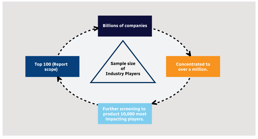
Step 1 - Identification of Relevant Samples Size from Population Database

Step 2 - Approaches for Defining Global Market Size (Value, Volume* & Price*)
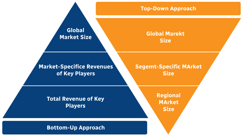
Note*: In applicable scenarios
Step 3 - Data Sources
Primary Research
- Web Analytics
- Survey Reports
- Research Institute
- Latest Research Reports
- Opinion Leaders
Secondary Research
- Annual Reports
- White Paper
- Latest Press Release
- Industry Association
- Paid Database
- Investor Presentations

Step 4 - Data Triangulation
Involves using different sources of information in order to increase the validity of a study
These sources are likely to be stakeholders in a program - participants, other researchers, program staff, other community members, and so on.
Then we put all data in single framework & apply various statistical tools to find out the dynamic on the market.
During the analysis stage, feedback from the stakeholder groups would be compared to determine areas of agreement as well as areas of divergence