

Key Insights
The semiconductor thin-film GaN epitaxial wafer market is poised for significant expansion, driven by the escalating demand for high-frequency, high-power, and energy-efficient electronic devices. This growth is propelled by the widespread adoption of Gallium Nitride (GaN) technology across critical sectors including 5G infrastructure, electric vehicles (EVs), renewable energy systems, and advanced power supplies. GaN's inherent superior performance characteristics over traditional silicon semiconductors enable the development of smaller, lighter, and more efficient electronic components. The market landscape is highly competitive, featuring a blend of established industry leaders and innovative emerging players actively contributing to technological advancements and increased production capabilities. Market segmentation is based on wafer diameter, material purity, and end-use applications, with distinct regional dynamics influencing adoption rates and manufacturing expertise. The market is projected to reach $3.88 billion by 2024, exhibiting a Compound Annual Growth Rate (CAGR) of 9.38% from the base year 2024.
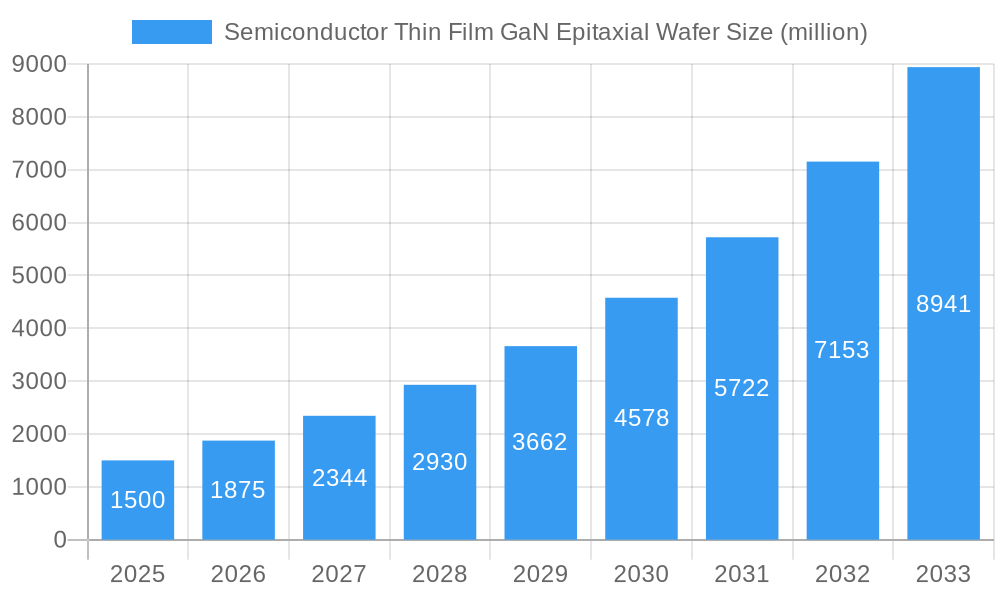
Semiconductor Thin Film GaN Epitaxial Wafer Market Size (In Billion)
Key market restraints include the comparatively higher cost of GaN wafers and the complexities associated with GaN fabrication. However, continuous advancements in manufacturing processes and the realization of economies of scale are progressively mitigating these challenges. A notable trend anticipated is the industry's shift towards larger diameter wafers, enhancing cost-effectiveness. Leading companies are actively pursuing strategic alliances, mergers and acquisitions, and capacity expansions to fortify their market standing and meet burgeoning demand. This evolving market environment is set to foster sustained growth and innovation, with a strategic emphasis on optimizing production to improve GaN's cost competitiveness and broaden its application spectrum across diverse industries.
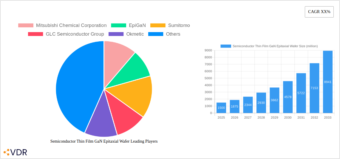
Semiconductor Thin Film GaN Epitaxial Wafer Company Market Share
Semiconductor Thin Film GaN Epitaxial Wafer Market Report: 2019-2033
This comprehensive report provides a detailed analysis of the semiconductor thin film GaN epitaxial wafer market, encompassing market dynamics, growth trends, regional analysis, product landscape, and key player profiles. The study period covers 2019-2033, with a base year of 2025 and a forecast period of 2025-2033. The report is essential for industry professionals, investors, and researchers seeking in-depth insights into this rapidly evolving sector of the wider semiconductor industry (parent market) and the power electronics market (child market).
Semiconductor Thin Film GaN Epitaxial Wafer Market Dynamics & Structure
This section analyzes the market concentration, technological innovation drivers, regulatory landscape, competitive substitutes, end-user demographics, and M&A activities within the semiconductor thin film GaN epitaxial wafer market. The market exhibits a moderately consolidated structure, with key players controlling xx% of the market share in 2025.
- Market Concentration: Moderate concentration, with top 5 players holding xx% market share in 2025.
- Technological Innovation: Continuous improvements in GaN material quality, wafer size, and cost-effectiveness drive innovation. Challenges include achieving higher yields and improving defect density.
- Regulatory Framework: Government initiatives promoting the adoption of GaN-based devices in various applications influence market growth.
- Competitive Substitutes: Silicon carbide (SiC) wafers present a competitive substitute, though GaN offers superior performance in specific applications.
- End-User Demographics: Growth is driven by diverse end-user segments, including power electronics, 5G infrastructure, RF applications, and automotive electronics.
- M&A Trends: The number of M&A deals in the GaN epitaxial wafer sector averaged xx per year during the historical period (2019-2024). Strategic acquisitions aimed to enhance production capacity and expand product portfolios are prevalent.
Semiconductor Thin Film GaN Epitaxial Wafer Growth Trends & Insights
The global semiconductor thin film GaN epitaxial wafer market witnessed significant growth during the historical period (2019-2024), expanding from xx million units in 2019 to xx million units in 2024. This growth is projected to continue with a Compound Annual Growth Rate (CAGR) of xx% during the forecast period (2025-2033), reaching an estimated xx million units by 2033. This expansion is fueled by increasing demand from various applications, advancements in GaN technology, and supportive government policies. The market penetration of GaN-based devices is increasing steadily across various sectors, further driving market growth. Technological disruptions, particularly in the area of high-power electronics and 5G infrastructure development, have accelerated adoption rates. Consumer behavior shifts toward energy-efficient and high-performance electronics are also significant factors.
Dominant Regions, Countries, or Segments in Semiconductor Thin Film GaN Epitaxial Wafer
The market is predominantly driven by Asia, particularly China, Japan, and South Korea, which account for xx% of the global market share in 2025. These regions benefit from robust manufacturing infrastructure, significant government investments in research and development, and strong demand from end-user sectors.
- Key Drivers in Asia:
- Strong government support for the semiconductor industry through subsidies and investment in research & development.
- Established manufacturing infrastructure and supply chain ecosystem.
- High demand for GaN-based devices from 5G infrastructure and consumer electronics sectors.
- North America and Europe: These regions show steady growth, driven by investments in renewable energy and electric vehicles, along with advancements in high-frequency applications.
Semiconductor Thin Film GaN Epitaxial Wafer Product Landscape
The market offers a range of semiconductor thin film GaN epitaxial wafers with varying sizes, thicknesses, and doping levels, optimized for different applications. Recent product innovations focus on enhanced crystal quality, larger wafer sizes, and improved defect density control. These advancements lead to improved device performance, higher yields, and reduced manufacturing costs. The unique selling propositions of these wafers include superior electron mobility, high breakdown voltage, and excellent thermal conductivity, making them suitable for power electronics and high-frequency applications.
Key Drivers, Barriers & Challenges in Semiconductor Thin Film GaN Epitaxial Wafer
Key Drivers:
- Rising demand from 5G infrastructure deployment.
- Growing adoption in electric vehicles and renewable energy systems.
- Technological advancements improving GaN wafer quality and reducing production costs.
Key Challenges:
- High manufacturing costs compared to silicon-based alternatives.
- Supply chain disruptions impacting the availability of raw materials.
- Competition from other wide-bandgap semiconductor materials like SiC. The cost disadvantage represents a significant barrier, limiting market penetration in price-sensitive applications.
Emerging Opportunities in Semiconductor Thin Film GaN Epitaxial Wafer
Significant opportunities exist in the untapped markets of developing economies, particularly in Asia and Africa. The expansion into new applications such as power inverters for electric vehicles, high-efficiency solar inverters, and advanced sensors offer substantial growth potential. Furthermore, the increasing demand for energy-efficient solutions in data centers and consumer electronics will continue to drive market expansion.
Growth Accelerators in the Semiconductor Thin Film GaN Epitaxial Wafer Industry
Long-term growth is fueled by continuous technological breakthroughs leading to improvements in GaN crystal quality, cost reductions, and the development of larger-diameter wafers. Strategic partnerships between manufacturers and end-users accelerate the adoption of GaN-based technologies. Furthermore, market expansion strategies targeting new application areas contribute to sustained growth.
Key Players Shaping the Semiconductor Thin Film GaN Epitaxial Wafer Market
- Mitsubishi Chemical Corporation
- EpiGaN
- Sumitomo
- GLC Semiconductor Group
- Okmetic
- IGSS GaN
- Homray Material Technology
- POWDEC K.K.
- Nitride Semiconductors
- Atecom Technology
- CorEnergy Semiconductor
- Air Water
- Ceramicforum
- Zhonghuan Semiconductor
- Xiamen Powerway Advanced Material
- Dongguan Sino Crystal Semiconductor
Notable Milestones in Semiconductor Thin Film GaN Epitaxial Wafer Sector
- 2020: Introduction of xx mm GaN wafers by [Company Name].
- 2021: Strategic partnership between [Company A] and [Company B] to develop next-generation GaN devices.
- 2022: Launch of high-power GaN epitaxial wafers with improved thermal conductivity by [Company Name].
- 2023: Successful commercialization of xx mm GaN wafers for power electronics applications.
- 2024: Acquisition of [Company A] by [Company B], expanding market share in GaN wafer production.
In-Depth Semiconductor Thin Film GaN Epitaxial Wafer Market Outlook
The future of the semiconductor thin film GaN epitaxial wafer market looks bright, driven by continued technological advancements, expanding applications, and growing demand across various sectors. Strategic partnerships and innovative market expansion strategies will further accelerate growth. The market is poised for significant expansion, presenting substantial opportunities for key players and new entrants alike.
Semiconductor Thin Film GaN Epitaxial Wafer Segmentation
-
1. Application
- 1.1. CATV
- 1.2. 5G Communications
- 1.3. Radars
- 1.4. Aerospace
- 1.5. Others
-
2. Types
- 2.1. Silicon Substrate
- 2.2. Sapphire Substrate
- 2.3. Silicon Carbide Substrate
Semiconductor Thin Film GaN Epitaxial Wafer Segmentation By Geography
-
1. North America
- 1.1. United States
- 1.2. Canada
- 1.3. Mexico
-
2. South America
- 2.1. Brazil
- 2.2. Argentina
- 2.3. Rest of South America
-
3. Europe
- 3.1. United Kingdom
- 3.2. Germany
- 3.3. France
- 3.4. Italy
- 3.5. Spain
- 3.6. Russia
- 3.7. Benelux
- 3.8. Nordics
- 3.9. Rest of Europe
-
4. Middle East & Africa
- 4.1. Turkey
- 4.2. Israel
- 4.3. GCC
- 4.4. North Africa
- 4.5. South Africa
- 4.6. Rest of Middle East & Africa
-
5. Asia Pacific
- 5.1. China
- 5.2. India
- 5.3. Japan
- 5.4. South Korea
- 5.5. ASEAN
- 5.6. Oceania
- 5.7. Rest of Asia Pacific
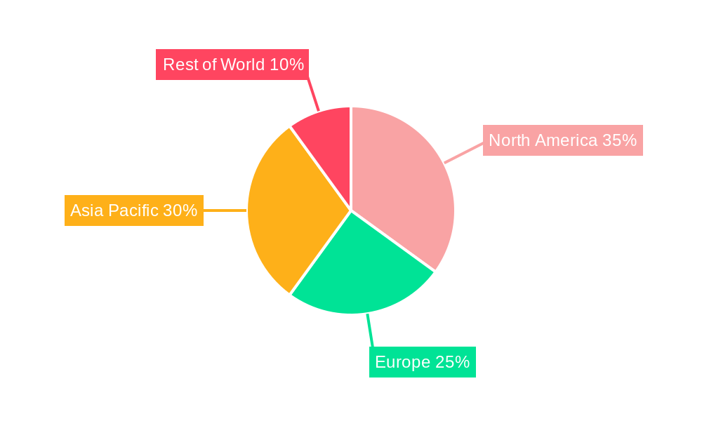
Semiconductor Thin Film GaN Epitaxial Wafer Regional Market Share
Geographic Coverage of Semiconductor Thin Film GaN Epitaxial Wafer
Semiconductor Thin Film GaN Epitaxial Wafer REPORT HIGHLIGHTS
| Aspects | Details |
|---|---|
| Study Period | 2020-2034 |
| Base Year | 2025 |
| Estimated Year | 2026 |
| Forecast Period | 2026-2034 |
| Historical Period | 2020-2025 |
| Growth Rate | CAGR of 9.38% from 2020-2034 |
| Segmentation |
|
Table of Contents
- 1. Introduction
- 1.1. Research Scope
- 1.2. Market Segmentation
- 1.3. Research Objective
- 1.4. Definitions and Assumptions
- 2. Executive Summary
- 2.1. Market Snapshot
- 3. Market Dynamics
- 3.1. Market Drivers
- 3.2. Market Restrains
- 3.3. Market Trends
- 3.4. Market Opportunities
- 4. Market Factor Analysis
- 4.1. Porters Five Forces
- 4.1.1. Bargaining Power of Suppliers
- 4.1.2. Bargaining Power of Buyers
- 4.1.3. Threat of New Entrants
- 4.1.4. Threat of Substitutes
- 4.1.5. Competitive Rivalry
- 4.2. PESTEL analysis
- 4.3. BCG Analysis
- 4.3.1. Stars (High Growth, High Market Share)
- 4.3.2. Cash Cows (Low Growth, High Market Share)
- 4.3.3. Question Mark (High Growth, Low Market Share)
- 4.3.4. Dogs (Low Growth, Low Market Share)
- 4.4. Ansoff Matrix Analysis
- 4.5. Supply Chain Analysis
- 4.6. Regulatory Landscape
- 4.7. Current Market Potential and Opportunity Assessment (TAM–SAM–SOM Framework)
- 4.8. VDR Analyst Note
- 4.1. Porters Five Forces
- 5. Market Analysis, Insights and Forecast 2021-2033
- 5.1. Market Analysis, Insights and Forecast - by Application
- 5.1.1. CATV
- 5.1.2. 5G Communications
- 5.1.3. Radars
- 5.1.4. Aerospace
- 5.1.5. Others
- 5.2. Market Analysis, Insights and Forecast - by Types
- 5.2.1. Silicon Substrate
- 5.2.2. Sapphire Substrate
- 5.2.3. Silicon Carbide Substrate
- 5.3. Market Analysis, Insights and Forecast - by Region
- 5.3.1. North America
- 5.3.2. South America
- 5.3.3. Europe
- 5.3.4. Middle East & Africa
- 5.3.5. Asia Pacific
- 5.1. Market Analysis, Insights and Forecast - by Application
- 6. Global Semiconductor Thin Film GaN Epitaxial Wafer Analysis, Insights and Forecast, 2021-2033
- 6.1. Market Analysis, Insights and Forecast - by Application
- 6.1.1. CATV
- 6.1.2. 5G Communications
- 6.1.3. Radars
- 6.1.4. Aerospace
- 6.1.5. Others
- 6.2. Market Analysis, Insights and Forecast - by Types
- 6.2.1. Silicon Substrate
- 6.2.2. Sapphire Substrate
- 6.2.3. Silicon Carbide Substrate
- 6.1. Market Analysis, Insights and Forecast - by Application
- 7. North America Semiconductor Thin Film GaN Epitaxial Wafer Analysis, Insights and Forecast, 2021-2033
- 7.1. Market Analysis, Insights and Forecast - by Application
- 7.1.1. CATV
- 7.1.2. 5G Communications
- 7.1.3. Radars
- 7.1.4. Aerospace
- 7.1.5. Others
- 7.2. Market Analysis, Insights and Forecast - by Types
- 7.2.1. Silicon Substrate
- 7.2.2. Sapphire Substrate
- 7.2.3. Silicon Carbide Substrate
- 7.1. Market Analysis, Insights and Forecast - by Application
- 8. South America Semiconductor Thin Film GaN Epitaxial Wafer Analysis, Insights and Forecast, 2021-2033
- 8.1. Market Analysis, Insights and Forecast - by Application
- 8.1.1. CATV
- 8.1.2. 5G Communications
- 8.1.3. Radars
- 8.1.4. Aerospace
- 8.1.5. Others
- 8.2. Market Analysis, Insights and Forecast - by Types
- 8.2.1. Silicon Substrate
- 8.2.2. Sapphire Substrate
- 8.2.3. Silicon Carbide Substrate
- 8.1. Market Analysis, Insights and Forecast - by Application
- 9. Europe Semiconductor Thin Film GaN Epitaxial Wafer Analysis, Insights and Forecast, 2021-2033
- 9.1. Market Analysis, Insights and Forecast - by Application
- 9.1.1. CATV
- 9.1.2. 5G Communications
- 9.1.3. Radars
- 9.1.4. Aerospace
- 9.1.5. Others
- 9.2. Market Analysis, Insights and Forecast - by Types
- 9.2.1. Silicon Substrate
- 9.2.2. Sapphire Substrate
- 9.2.3. Silicon Carbide Substrate
- 9.1. Market Analysis, Insights and Forecast - by Application
- 10. Middle East & Africa Semiconductor Thin Film GaN Epitaxial Wafer Analysis, Insights and Forecast, 2021-2033
- 10.1. Market Analysis, Insights and Forecast - by Application
- 10.1.1. CATV
- 10.1.2. 5G Communications
- 10.1.3. Radars
- 10.1.4. Aerospace
- 10.1.5. Others
- 10.2. Market Analysis, Insights and Forecast - by Types
- 10.2.1. Silicon Substrate
- 10.2.2. Sapphire Substrate
- 10.2.3. Silicon Carbide Substrate
- 10.1. Market Analysis, Insights and Forecast - by Application
- 11. Asia Pacific Semiconductor Thin Film GaN Epitaxial Wafer Analysis, Insights and Forecast, 2021-2033
- 11.1. Market Analysis, Insights and Forecast - by Application
- 11.1.1. CATV
- 11.1.2. 5G Communications
- 11.1.3. Radars
- 11.1.4. Aerospace
- 11.1.5. Others
- 11.2. Market Analysis, Insights and Forecast - by Types
- 11.2.1. Silicon Substrate
- 11.2.2. Sapphire Substrate
- 11.2.3. Silicon Carbide Substrate
- 11.1. Market Analysis, Insights and Forecast - by Application
- 12. Competitive Analysis
- 12.1. Company Profiles
- 12.1.1 Mitsubishi Chemical Corporation
- 12.1.1.1. Company Overview
- 12.1.1.2. Products
- 12.1.1.3. Company Financials
- 12.1.1.4. SWOT Analysis
- 12.1.2 EpiGaN
- 12.1.2.1. Company Overview
- 12.1.2.2. Products
- 12.1.2.3. Company Financials
- 12.1.2.4. SWOT Analysis
- 12.1.3 Sumitomo
- 12.1.3.1. Company Overview
- 12.1.3.2. Products
- 12.1.3.3. Company Financials
- 12.1.3.4. SWOT Analysis
- 12.1.4 GLC Semiconductor Group
- 12.1.4.1. Company Overview
- 12.1.4.2. Products
- 12.1.4.3. Company Financials
- 12.1.4.4. SWOT Analysis
- 12.1.5 Okmetic
- 12.1.5.1. Company Overview
- 12.1.5.2. Products
- 12.1.5.3. Company Financials
- 12.1.5.4. SWOT Analysis
- 12.1.6 IGSS GaN
- 12.1.6.1. Company Overview
- 12.1.6.2. Products
- 12.1.6.3. Company Financials
- 12.1.6.4. SWOT Analysis
- 12.1.7 Homray Material Technology
- 12.1.7.1. Company Overview
- 12.1.7.2. Products
- 12.1.7.3. Company Financials
- 12.1.7.4. SWOT Analysis
- 12.1.8 POWDEC K.K.
- 12.1.8.1. Company Overview
- 12.1.8.2. Products
- 12.1.8.3. Company Financials
- 12.1.8.4. SWOT Analysis
- 12.1.9 Nitride Semiconductors
- 12.1.9.1. Company Overview
- 12.1.9.2. Products
- 12.1.9.3. Company Financials
- 12.1.9.4. SWOT Analysis
- 12.1.10 Atecom Technology
- 12.1.10.1. Company Overview
- 12.1.10.2. Products
- 12.1.10.3. Company Financials
- 12.1.10.4. SWOT Analysis
- 12.1.11 CorEnergy Semiconductor
- 12.1.11.1. Company Overview
- 12.1.11.2. Products
- 12.1.11.3. Company Financials
- 12.1.11.4. SWOT Analysis
- 12.1.12 Air Water
- 12.1.12.1. Company Overview
- 12.1.12.2. Products
- 12.1.12.3. Company Financials
- 12.1.12.4. SWOT Analysis
- 12.1.13 Ceramicforum
- 12.1.13.1. Company Overview
- 12.1.13.2. Products
- 12.1.13.3. Company Financials
- 12.1.13.4. SWOT Analysis
- 12.1.14 Zhonghuan Semiconductor
- 12.1.14.1. Company Overview
- 12.1.14.2. Products
- 12.1.14.3. Company Financials
- 12.1.14.4. SWOT Analysis
- 12.1.15 Xiamen Powerway Advanced Material
- 12.1.15.1. Company Overview
- 12.1.15.2. Products
- 12.1.15.3. Company Financials
- 12.1.15.4. SWOT Analysis
- 12.1.16 Dongguan Sino Crystal Semiconductor
- 12.1.16.1. Company Overview
- 12.1.16.2. Products
- 12.1.16.3. Company Financials
- 12.1.16.4. SWOT Analysis
- 12.1.1 Mitsubishi Chemical Corporation
- 12.2. Market Entropy
- 12.2.1 Company's Key Areas Served
- 12.2.2 Recent Developments
- 12.3. Company Market Share Analysis 2025
- 12.3.1 Top 5 Companies Market Share Analysis
- 12.3.2 Top 3 Companies Market Share Analysis
- 12.4. List of Potential Customers
- 13. Research Methodology
List of Figures
- Figure 1: Global Semiconductor Thin Film GaN Epitaxial Wafer Revenue Breakdown (billion, %) by Region 2025 & 2033
- Figure 2: North America Semiconductor Thin Film GaN Epitaxial Wafer Revenue (billion), by Application 2025 & 2033
- Figure 3: North America Semiconductor Thin Film GaN Epitaxial Wafer Revenue Share (%), by Application 2025 & 2033
- Figure 4: North America Semiconductor Thin Film GaN Epitaxial Wafer Revenue (billion), by Types 2025 & 2033
- Figure 5: North America Semiconductor Thin Film GaN Epitaxial Wafer Revenue Share (%), by Types 2025 & 2033
- Figure 6: North America Semiconductor Thin Film GaN Epitaxial Wafer Revenue (billion), by Country 2025 & 2033
- Figure 7: North America Semiconductor Thin Film GaN Epitaxial Wafer Revenue Share (%), by Country 2025 & 2033
- Figure 8: South America Semiconductor Thin Film GaN Epitaxial Wafer Revenue (billion), by Application 2025 & 2033
- Figure 9: South America Semiconductor Thin Film GaN Epitaxial Wafer Revenue Share (%), by Application 2025 & 2033
- Figure 10: South America Semiconductor Thin Film GaN Epitaxial Wafer Revenue (billion), by Types 2025 & 2033
- Figure 11: South America Semiconductor Thin Film GaN Epitaxial Wafer Revenue Share (%), by Types 2025 & 2033
- Figure 12: South America Semiconductor Thin Film GaN Epitaxial Wafer Revenue (billion), by Country 2025 & 2033
- Figure 13: South America Semiconductor Thin Film GaN Epitaxial Wafer Revenue Share (%), by Country 2025 & 2033
- Figure 14: Europe Semiconductor Thin Film GaN Epitaxial Wafer Revenue (billion), by Application 2025 & 2033
- Figure 15: Europe Semiconductor Thin Film GaN Epitaxial Wafer Revenue Share (%), by Application 2025 & 2033
- Figure 16: Europe Semiconductor Thin Film GaN Epitaxial Wafer Revenue (billion), by Types 2025 & 2033
- Figure 17: Europe Semiconductor Thin Film GaN Epitaxial Wafer Revenue Share (%), by Types 2025 & 2033
- Figure 18: Europe Semiconductor Thin Film GaN Epitaxial Wafer Revenue (billion), by Country 2025 & 2033
- Figure 19: Europe Semiconductor Thin Film GaN Epitaxial Wafer Revenue Share (%), by Country 2025 & 2033
- Figure 20: Middle East & Africa Semiconductor Thin Film GaN Epitaxial Wafer Revenue (billion), by Application 2025 & 2033
- Figure 21: Middle East & Africa Semiconductor Thin Film GaN Epitaxial Wafer Revenue Share (%), by Application 2025 & 2033
- Figure 22: Middle East & Africa Semiconductor Thin Film GaN Epitaxial Wafer Revenue (billion), by Types 2025 & 2033
- Figure 23: Middle East & Africa Semiconductor Thin Film GaN Epitaxial Wafer Revenue Share (%), by Types 2025 & 2033
- Figure 24: Middle East & Africa Semiconductor Thin Film GaN Epitaxial Wafer Revenue (billion), by Country 2025 & 2033
- Figure 25: Middle East & Africa Semiconductor Thin Film GaN Epitaxial Wafer Revenue Share (%), by Country 2025 & 2033
- Figure 26: Asia Pacific Semiconductor Thin Film GaN Epitaxial Wafer Revenue (billion), by Application 2025 & 2033
- Figure 27: Asia Pacific Semiconductor Thin Film GaN Epitaxial Wafer Revenue Share (%), by Application 2025 & 2033
- Figure 28: Asia Pacific Semiconductor Thin Film GaN Epitaxial Wafer Revenue (billion), by Types 2025 & 2033
- Figure 29: Asia Pacific Semiconductor Thin Film GaN Epitaxial Wafer Revenue Share (%), by Types 2025 & 2033
- Figure 30: Asia Pacific Semiconductor Thin Film GaN Epitaxial Wafer Revenue (billion), by Country 2025 & 2033
- Figure 31: Asia Pacific Semiconductor Thin Film GaN Epitaxial Wafer Revenue Share (%), by Country 2025 & 2033
List of Tables
- Table 1: Global Semiconductor Thin Film GaN Epitaxial Wafer Revenue billion Forecast, by Application 2020 & 2033
- Table 2: Global Semiconductor Thin Film GaN Epitaxial Wafer Revenue billion Forecast, by Types 2020 & 2033
- Table 3: Global Semiconductor Thin Film GaN Epitaxial Wafer Revenue billion Forecast, by Region 2020 & 2033
- Table 4: Global Semiconductor Thin Film GaN Epitaxial Wafer Revenue billion Forecast, by Application 2020 & 2033
- Table 5: Global Semiconductor Thin Film GaN Epitaxial Wafer Revenue billion Forecast, by Types 2020 & 2033
- Table 6: Global Semiconductor Thin Film GaN Epitaxial Wafer Revenue billion Forecast, by Country 2020 & 2033
- Table 7: United States Semiconductor Thin Film GaN Epitaxial Wafer Revenue (billion) Forecast, by Application 2020 & 2033
- Table 8: Canada Semiconductor Thin Film GaN Epitaxial Wafer Revenue (billion) Forecast, by Application 2020 & 2033
- Table 9: Mexico Semiconductor Thin Film GaN Epitaxial Wafer Revenue (billion) Forecast, by Application 2020 & 2033
- Table 10: Global Semiconductor Thin Film GaN Epitaxial Wafer Revenue billion Forecast, by Application 2020 & 2033
- Table 11: Global Semiconductor Thin Film GaN Epitaxial Wafer Revenue billion Forecast, by Types 2020 & 2033
- Table 12: Global Semiconductor Thin Film GaN Epitaxial Wafer Revenue billion Forecast, by Country 2020 & 2033
- Table 13: Brazil Semiconductor Thin Film GaN Epitaxial Wafer Revenue (billion) Forecast, by Application 2020 & 2033
- Table 14: Argentina Semiconductor Thin Film GaN Epitaxial Wafer Revenue (billion) Forecast, by Application 2020 & 2033
- Table 15: Rest of South America Semiconductor Thin Film GaN Epitaxial Wafer Revenue (billion) Forecast, by Application 2020 & 2033
- Table 16: Global Semiconductor Thin Film GaN Epitaxial Wafer Revenue billion Forecast, by Application 2020 & 2033
- Table 17: Global Semiconductor Thin Film GaN Epitaxial Wafer Revenue billion Forecast, by Types 2020 & 2033
- Table 18: Global Semiconductor Thin Film GaN Epitaxial Wafer Revenue billion Forecast, by Country 2020 & 2033
- Table 19: United Kingdom Semiconductor Thin Film GaN Epitaxial Wafer Revenue (billion) Forecast, by Application 2020 & 2033
- Table 20: Germany Semiconductor Thin Film GaN Epitaxial Wafer Revenue (billion) Forecast, by Application 2020 & 2033
- Table 21: France Semiconductor Thin Film GaN Epitaxial Wafer Revenue (billion) Forecast, by Application 2020 & 2033
- Table 22: Italy Semiconductor Thin Film GaN Epitaxial Wafer Revenue (billion) Forecast, by Application 2020 & 2033
- Table 23: Spain Semiconductor Thin Film GaN Epitaxial Wafer Revenue (billion) Forecast, by Application 2020 & 2033
- Table 24: Russia Semiconductor Thin Film GaN Epitaxial Wafer Revenue (billion) Forecast, by Application 2020 & 2033
- Table 25: Benelux Semiconductor Thin Film GaN Epitaxial Wafer Revenue (billion) Forecast, by Application 2020 & 2033
- Table 26: Nordics Semiconductor Thin Film GaN Epitaxial Wafer Revenue (billion) Forecast, by Application 2020 & 2033
- Table 27: Rest of Europe Semiconductor Thin Film GaN Epitaxial Wafer Revenue (billion) Forecast, by Application 2020 & 2033
- Table 28: Global Semiconductor Thin Film GaN Epitaxial Wafer Revenue billion Forecast, by Application 2020 & 2033
- Table 29: Global Semiconductor Thin Film GaN Epitaxial Wafer Revenue billion Forecast, by Types 2020 & 2033
- Table 30: Global Semiconductor Thin Film GaN Epitaxial Wafer Revenue billion Forecast, by Country 2020 & 2033
- Table 31: Turkey Semiconductor Thin Film GaN Epitaxial Wafer Revenue (billion) Forecast, by Application 2020 & 2033
- Table 32: Israel Semiconductor Thin Film GaN Epitaxial Wafer Revenue (billion) Forecast, by Application 2020 & 2033
- Table 33: GCC Semiconductor Thin Film GaN Epitaxial Wafer Revenue (billion) Forecast, by Application 2020 & 2033
- Table 34: North Africa Semiconductor Thin Film GaN Epitaxial Wafer Revenue (billion) Forecast, by Application 2020 & 2033
- Table 35: South Africa Semiconductor Thin Film GaN Epitaxial Wafer Revenue (billion) Forecast, by Application 2020 & 2033
- Table 36: Rest of Middle East & Africa Semiconductor Thin Film GaN Epitaxial Wafer Revenue (billion) Forecast, by Application 2020 & 2033
- Table 37: Global Semiconductor Thin Film GaN Epitaxial Wafer Revenue billion Forecast, by Application 2020 & 2033
- Table 38: Global Semiconductor Thin Film GaN Epitaxial Wafer Revenue billion Forecast, by Types 2020 & 2033
- Table 39: Global Semiconductor Thin Film GaN Epitaxial Wafer Revenue billion Forecast, by Country 2020 & 2033
- Table 40: China Semiconductor Thin Film GaN Epitaxial Wafer Revenue (billion) Forecast, by Application 2020 & 2033
- Table 41: India Semiconductor Thin Film GaN Epitaxial Wafer Revenue (billion) Forecast, by Application 2020 & 2033
- Table 42: Japan Semiconductor Thin Film GaN Epitaxial Wafer Revenue (billion) Forecast, by Application 2020 & 2033
- Table 43: South Korea Semiconductor Thin Film GaN Epitaxial Wafer Revenue (billion) Forecast, by Application 2020 & 2033
- Table 44: ASEAN Semiconductor Thin Film GaN Epitaxial Wafer Revenue (billion) Forecast, by Application 2020 & 2033
- Table 45: Oceania Semiconductor Thin Film GaN Epitaxial Wafer Revenue (billion) Forecast, by Application 2020 & 2033
- Table 46: Rest of Asia Pacific Semiconductor Thin Film GaN Epitaxial Wafer Revenue (billion) Forecast, by Application 2020 & 2033
Frequently Asked Questions
1. What is the projected Compound Annual Growth Rate (CAGR) of the Semiconductor Thin Film GaN Epitaxial Wafer?
The projected CAGR is approximately 9.38%.
2. Which companies are prominent players in the Semiconductor Thin Film GaN Epitaxial Wafer?
Key companies in the market include Mitsubishi Chemical Corporation, EpiGaN, Sumitomo, GLC Semiconductor Group, Okmetic, IGSS GaN, Homray Material Technology, POWDEC K.K., Nitride Semiconductors, Atecom Technology, CorEnergy Semiconductor, Air Water, Ceramicforum, Zhonghuan Semiconductor, Xiamen Powerway Advanced Material, Dongguan Sino Crystal Semiconductor.
3. What are the main segments of the Semiconductor Thin Film GaN Epitaxial Wafer?
The market segments include Application, Types.
4. Can you provide details about the market size?
The market size is estimated to be USD 3.88 billion as of 2022.
5. What are some drivers contributing to market growth?
N/A
6. What are the notable trends driving market growth?
N/A
7. Are there any restraints impacting market growth?
N/A
8. Can you provide examples of recent developments in the market?
N/A
9. What pricing options are available for accessing the report?
Pricing options include single-user, multi-user, and enterprise licenses priced at USD 2900.00, USD 4350.00, and USD 5800.00 respectively.
10. Is the market size provided in terms of value or volume?
The market size is provided in terms of value, measured in billion.
11. Are there any specific market keywords associated with the report?
Yes, the market keyword associated with the report is "Semiconductor Thin Film GaN Epitaxial Wafer," which aids in identifying and referencing the specific market segment covered.
12. How do I determine which pricing option suits my needs best?
The pricing options vary based on user requirements and access needs. Individual users may opt for single-user licenses, while businesses requiring broader access may choose multi-user or enterprise licenses for cost-effective access to the report.
13. Are there any additional resources or data provided in the Semiconductor Thin Film GaN Epitaxial Wafer report?
While the report offers comprehensive insights, it's advisable to review the specific contents or supplementary materials provided to ascertain if additional resources or data are available.
14. How can I stay updated on further developments or reports in the Semiconductor Thin Film GaN Epitaxial Wafer?
To stay informed about further developments, trends, and reports in the Semiconductor Thin Film GaN Epitaxial Wafer, consider subscribing to industry newsletters, following relevant companies and organizations, or regularly checking reputable industry news sources and publications.
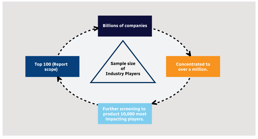
Methodology
Step 1 - Identification of Relevant Samples Size from Population Database

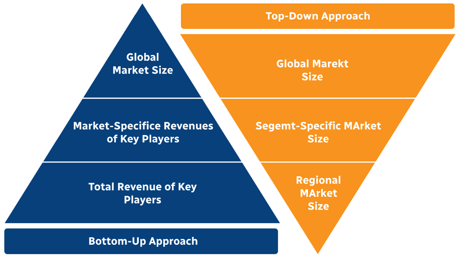
Step 2 - Approaches for Defining Global Market Size (Value, Volume* & Price*)
Note*: In applicable scenarios
Step 3 - Data Sources
Primary Research
- Web Analytics
- Survey Reports
- Research Institute
- Latest Research Reports
- Opinion Leaders
Secondary Research
- Annual Reports
- White Paper
- Latest Press Release
- Industry Association
- Paid Database
- Investor Presentations

Step 4 - Data Triangulation
Involves using different sources of information in order to increase the validity of a study
These sources are likely to be stakeholders in a program - participants, other researchers, program staff, other community members, and so on.
Then we put all data in single framework & apply various statistical tools to find out the dynamic on the market.
During the analysis stage, feedback from the stakeholder groups would be compared to determine areas of agreement as well as areas of divergence