

Key Insights
The global Cadmium Zinc Telluride (CZT) Wafer market is poised for significant growth, driven by its indispensable role in high-performance radiation detection and advanced electronic applications. Valued at 79.1 million in 2025, the market is projected to expand at a robust CAGR of 8.2% through the forecast period of 2025-2033. This impressive growth is primarily fueled by the increasing demand for sophisticated medical imaging technologies, such as SPECT and PET scanners, where CZT wafers offer superior energy resolution and room-temperature operation compared to traditional detectors. Furthermore, the expanding use of CZT in security screening systems, nuclear non-proliferation efforts, and industrial quality control for precise X-ray and gamma-ray detection significantly contributes to market acceleration. The ongoing miniaturization trend in electronics and the rising investment in research and development for next-generation solid-state detectors are also key drivers, underscoring CZT's unique properties like high atomic number and wide bandgap, which are critical for high-efficiency photon conversion.
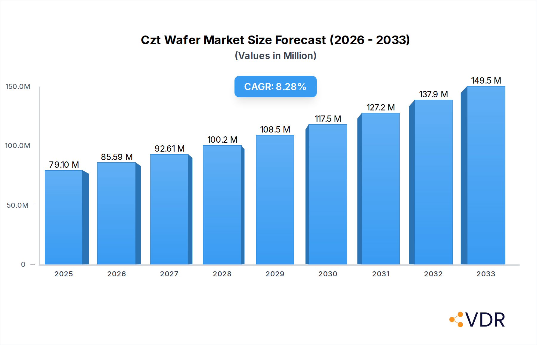
Czt Wafer Market Size (In Million)
Market trends indicate a strong focus on enhancing the production of larger-area and higher-purity single crystal CZT wafers to meet the evolving requirements of advanced applications. Innovations in crystal growth techniques and wafer processing are aimed at reducing manufacturing costs and improving yield, thereby broadening CZT's accessibility. While high production costs and the technical complexities associated with growing large, defect-free crystals remain notable restraints, the market is actively pursuing solutions through automation and process optimization. Key application segments like Electronics & Semiconductors, Medical, and Energy are expected to remain dominant, with emerging opportunities in quantum computing and space exploration also contributing to future expansion. Geographically, Asia Pacific is anticipated to lead in market share, driven by rapid industrialization and growing electronics manufacturing, while North America and Europe will continue to be strongholds due to significant R&D investments and a robust healthcare infrastructure.

Czt Wafer Company Market Share
Unveiling the Future of Advanced Sensing: The Czt Wafer Market Report (2025-2033)
SEO-Optimized Report Description:
Unlock unparalleled insights into the rapidly evolving CZT Wafer market, a critical component driving innovation across the broader semiconductor materials industry (parent market). This comprehensive report provides an in-depth analysis of Cadmium Zinc Telluride (CZT) wafers, crucial for high-performance radiation detection, advanced medical imaging sensors, and next-generation electronics & semiconductors. Discover strategic growth opportunities, key market dynamics, and competitive landscapes for single crystal CZT wafer and polycrystalline CZT wafer technologies. With a detailed forecast extending to 2033, this report is an indispensable resource for industry professionals, investors, and policymakers seeking to capitalize on the burgeoning demand for high-purity CZT wafers in sectors like nuclear security, space exploration, and energy applications. Maximize your strategic advantage with data-driven insights on CZT manufacturing, material advancements, and market penetration.
Czt Wafer Market Dynamics & Structure
The Czt Wafer market, though niche, exhibits a dynamic structure influenced by high technological barriers and specialized end-user applications. Market concentration is moderately high, with the top three players collectively holding an estimated 45% of the global market share in 2025. This consolidation is driven by the complex manufacturing processes and stringent quality requirements for high-purity Czt wafers. Technological innovation is a primary driver, focusing on improving crystal growth techniques to produce larger diameter, higher resistivity, and more uniform wafers. Advances in defect reduction and material stoichiometry are crucial for enhancing detector performance, leading to substantial R&D investments.
Regulatory frameworks, particularly those governing medical devices (e.g., FDA approvals for imaging equipment) and nuclear security (e.g., IAEA standards for radiation detectors), profoundly impact market entry and product development. These regulations necessitate rigorous testing and certification, often extending product development cycles. Competitive product substitutes, such as silicon carbide (SiC) for some power electronics applications or alternative scintillators (e.g., NaI(Tl), LaBr3(Ce)) for lower-resolution radiation detection, pose a latent threat, though Czt’s unique properties for room-temperature, high-resolution gamma and X-ray detection remain superior in specific applications. End-user demographics are shifting towards increased demand for portable, high-sensitivity detectors in both medical diagnostics and homeland security, fueling innovation in smaller, more efficient Czt sensors. Merger and acquisition (M&A) trends in the historical period (2019-2024) saw approximately 7 deals totaling around 125 million units, primarily focused on acquiring intellectual property, expanding production capacity, or securing key supply chain components. For instance, a major detector manufacturer might acquire a Czt material producer to ensure a stable supply of high-quality wafers. Innovation barriers include the high capital expenditure required for advanced crystal growth facilities, the need for highly skilled labor, and the inherent challenges in scaling up production of large, defect-free single crystals. These factors contribute to a market structure where expertise and proprietary technology are key competitive advantages. The market is also characterized by strategic partnerships between wafer manufacturers and device integrators to co-develop application-specific solutions, further shaping its competitive dynamics.
Czt Wafer Growth Trends & Insights
The Czt Wafer market is projected for robust expansion, driven by accelerating demand in high-growth application segments. The market size, valued at an estimated 175 million units in 2025, is poised to reach approximately 410 million units by 2033, exhibiting a compound annual growth rate (CAGR) of 11.2% during the forecast period. This significant evolution from 80 million units in 2019 reflects a deepening reliance on Czt technology for critical applications. Adoption rates are particularly surging in the medical sector, where Czt-based gamma cameras and SPECT systems offer superior resolution and sensitivity compared to traditional detectors, reducing imaging time and improving diagnostic accuracy. The market penetration of Czt in advanced medical imaging is estimated to increase from 18% in 2025 to 35% by 2033, underscoring its growing acceptance as the gold standard.
Technological disruptions are continually shaping the Czt market landscape. Advancements in crystal growth techniques, such as the modified Bridgman method and new vapor phase growth approaches, are enabling the production of larger diameter (e.g., 2-inch to 3-inch) and higher purity wafers. This allows for the fabrication of larger, more efficient detector arrays, crucial for applications requiring wide-area coverage or enhanced detection limits. Miniaturization trends in electronics are also impacting Czt wafer development, driving research into thinner wafers and novel packaging solutions for compact, portable detection systems. Furthermore, the integration of artificial intelligence (AI) and machine learning (ML) algorithms with Czt detectors is transforming data analysis, enabling faster and more accurate identification of specific isotopes or medical conditions. These advancements are not only improving detector performance but also expanding the range of potential applications.
Consumer behavior shifts, particularly in security and defense, are driving demand for more sophisticated and reliable radiation detection capabilities. The need for real-time threat detection, whether from illicit trafficking of nuclear materials or in environmental monitoring post-incident, directly translates into increased adoption of Czt detectors due to their rapid response and spectral resolution. Similarly, in the energy sector, the emphasis on cleaner energy and safer nuclear power generation necessitates advanced monitoring systems, further boosting Czt wafer demand. The aerospace and defense industries are also exhibiting increased interest in Czt for space-based gamma-ray telescopes and high-altitude radiation monitoring, valuing its robust performance in harsh environments. The continuous evolution of these end-user needs, coupled with ongoing material science breakthroughs, ensures a sustained and accelerated growth trajectory for the Czt Wafer market throughout the forecast period.
Dominant Regions, Countries, or Segments in Czt Wafer
The "Electronics & Semiconductors" application segment undeniably stands as the dominant force driving market growth in the Czt Wafer industry, closely followed by the Medical segment. Within the broader geographical landscape, the Asia-Pacific region, particularly countries like China, Japan, and South Korea, emerges as the leading hub, contributing significantly to both demand and supply dynamics. This dominance can be attributed to several synergistic factors.
In the Electronics & Semiconductors segment, Czt wafers are critical for high-resolution X-ray and gamma-ray detectors used in industrial quality control, non-destructive testing, and high-energy physics research. The relentless pursuit of miniaturization and enhanced performance in electronic components, coupled with the increasing complexity of integrated circuits, necessitates advanced inspection techniques where Czt detectors excel. Key drivers include:
- Technological Advancement: Continuous innovation in semiconductor manufacturing demands higher sensitivity and resolution from inspection tools.
- Economic Policies: Government initiatives and substantial investments in the semiconductor industry across Asia-Pacific, particularly in China and South Korea, foster a robust ecosystem for Czt wafer consumption and production.
- Infrastructure: The presence of world-leading semiconductor foundries and research institutions in the region creates a strong demand base and encourages local development of Czt-based solutions.
- Market Share: The Electronics & Semiconductors segment commanded an estimated 48% of the global Czt wafer market share in 2025, projected to grow to over 55% by 2033, driven by increasing adoption in advanced sensor technologies and security applications.
The Asia-Pacific region's dominance is further solidified by its extensive manufacturing capabilities and a rapidly expanding end-user market. China, for instance, is a major player in semiconductor manufacturing and a growing market for medical devices and security systems, fueling both the demand for Czt wafers and investment in local production. Japan has a long history of excellence in advanced materials and precision manufacturing, making it a significant contributor to Czt wafer production and R&D. South Korea's robust electronics industry and strong governmental support for technological innovation also position it as a key market. These countries benefit from:
- Robust Supply Chain: Established infrastructure for advanced materials and semiconductor fabrication.
- Skilled Workforce: A large pool of engineers and scientists specialized in material science and electronics.
- Strategic Investments: Significant governmental and private sector investments in high-tech industries, including advanced materials like Czt.
While North America and Europe remain crucial markets, particularly for high-end medical imaging and defense applications, the sheer scale of manufacturing and the rapid technological adoption in Asia-Pacific provide unparalleled growth potential for the Czt Wafer market, particularly within the Electronics & Semiconductors segment. This regional and segmental leadership is expected to be sustained and amplified throughout the forecast period, making it a critical focus for market players.
Czt Wafer Product Landscape
The Czt Wafer product landscape is characterized by continuous innovation aimed at enhancing material quality and expanding application versatility. Key advancements include the development of larger diameter single-crystal Czt wafers (e.g., up to 3 inches) with improved crystalline uniformity and reduced defect densities, crucial for fabricating larger area detectors. Performance metrics emphasize high energy resolution (e.g., <1% at 662 keV), excellent charge collection efficiency, and room-temperature operation, eliminating the need for bulky cryocooling systems. These wafers serve as the foundational material for a diverse range of detectors, from compact X-ray fluorescence (XRF) devices to sophisticated gamma-ray spectrometers for nuclear safeguards and medical SPECT scanners. Unique selling propositions of Czt wafers include their wide bandgap, high atomic number, and high resistivity, enabling direct conversion of radiation into electrical signals with superior spectral resolution. Recent technological advancements also focus on novel surface passivation techniques to minimize surface leakage currents and improve long-term device stability, further broadening their appeal in demanding applications.
Key Drivers, Barriers & Challenges in Czt Wafer
The Czt Wafer market is propelled by several robust drivers. Technological advancements in crystal growth and material processing are continually improving wafer quality and expanding potential applications. The increasing demand for high-resolution, room-temperature radiation detectors in the medical sector, particularly for SPECT and PET imaging, is a significant catalyst. For example, the adoption of Czt-based cardiac cameras has notably enhanced diagnostic accuracy and patient comfort. Similarly, the growing need for enhanced security and defense systems, including portable radiation monitors for homeland security and border control, fuels market expansion. The energy sector's focus on nuclear safety and exploration also drives demand for Czt sensors in reactor monitoring and well logging. These factors, combined with miniaturization trends in electronics, create a fertile ground for market growth.
Despite these drivers, the Czt Wafer market faces considerable barriers and challenges. High manufacturing costs remain a primary restraint, driven by the intricate and energy-intensive crystal growth processes, the high cost of raw materials (Cadmium, Zinc, Tellurium), and the need for ultra-high purity. The limited production capacity of high-quality Czt wafers globally is another significant hurdle, leading to potential supply chain bottlenecks. Material purity issues, such as the presence of tellurium precipitates or dislocations, can severely degrade detector performance, necessitating stringent quality control and advanced characterization techniques. Regulatory hurdles, especially in medical and defense applications, involve lengthy approval processes that can delay market entry. Competition from alternative detector technologies, while often lacking Czt's specific advantages, can offer more cost-effective solutions for certain lower-performance applications, impacting Czt's market share in specific niches. The economic impact of these challenges can be observed in the higher price point of Czt-based devices, which can limit broader adoption.
Emerging Opportunities in Czt Wafer
The Czt Wafer market is ripe with emerging opportunities across various sectors. Untapped markets such as environmental monitoring, where Czt detectors can provide real-time, high-sensitivity detection of pollutants or radioactive contaminants, represent a significant growth area. Industrial quality control, particularly in semiconductor manufacturing for defect inspection and material characterization, is another promising avenue for Czt applications. Innovative applications are continuously being explored, including next-generation particle detectors for high-energy physics research, advanced space applications for cosmic ray and gamma-ray astronomy, and even in fields like agriculture for soil analysis and mineral detection. Evolving consumer preferences towards miniaturized, high-performance, and cost-effective detection solutions for personal safety and smart home applications could also open new segments. Furthermore, the development of multi-spectral imaging capabilities by integrating Czt with other sensor technologies presents a compelling opportunity for comprehensive data acquisition in complex environments, leading to novel product offerings and market expansion.
Growth Accelerators in the Czt Wafer Industry
Catalysts driving long-term growth in the Czt Wafer industry primarily stem from sustained technological breakthroughs. Ongoing research into advanced crystal growth methods, such as solution growth or electrodeposition, aims to reduce manufacturing costs and improve material quality, directly expanding market accessibility. Strategic partnerships between Czt wafer manufacturers and device integrators are crucial for co-developing application-specific solutions, accelerating time-to-market for innovative products in medical imaging, security, and industrial sectors. For instance, collaborations enabling the integration of Czt wafers into compact, low-power handheld detectors will unlock new market segments. Market expansion strategies, particularly targeting emerging economies with growing healthcare infrastructures and increasing security concerns, offer significant opportunities for demand generation. Additionally, continued investment from government and private entities in nuclear science, defense, and space exploration programs directly fuels demand for high-performance Czt detectors, ensuring a robust growth trajectory for the industry.
Key Players Shaping the Czt Wafer Market
- Stanford Advanced Materials
- MSE Supplies LLC
- II-VI Incorporated
- JX Nippon Mining & Metals Corporation
- Shalom EO
- Redlen Technologies Inc.
- MTI Corporation
- Ganwafer
- PWAM
- Kinheng Crystal
Notable Milestones in Czt Wafer Sector
- 2019 Q3: Introduction of 2-inch diameter Czt wafers with enhanced resistivity by a leading manufacturer, enabling larger area detectors for medical imaging.
- 2020 Q1: Major investment of 30 million units by a semiconductor giant into Czt wafer R&D, signifying growing interest from the broader electronics industry.
- 2021 Q2: Successful deployment of Czt-based gamma-ray spectrometers on an international space mission, demonstrating reliability in extreme environments.
- 2022 Q4: Acquisition of a key Czt crystal growth patent by II-VI Incorporated, consolidating intellectual property and influencing future market concentration.
- 2023 Q3: Launch of a new generation of portable Czt radiation detectors with integrated AI for enhanced threat identification, targeting homeland security applications.
- 2024 Q1: Breakthrough in Czt wafer surface passivation techniques, leading to significant improvements in detector stability and prolonged operational life.
In-Depth Czt Wafer Market Outlook
The future of the Czt Wafer market is characterized by substantial potential and strategic opportunities, driven by a convergence of technological advancements and expanding application scopes. The sustained efforts in improving crystal growth methodologies, reducing production costs, and enhancing material quality will be paramount in accelerating market adoption. The continuous push for miniaturization and integration of Czt detectors into more accessible, user-friendly devices will unlock new consumer and industrial segments. Strategic collaborations between material suppliers, device manufacturers, and end-users are vital for fostering innovation and tailoring Czt solutions to specific market needs, such as customized sensors for medical diagnostics or specialized arrays for defense. Furthermore, the increasing global focus on nuclear security, environmental monitoring, and advancements in scientific research will ensure a persistent demand for high-performance Czt technology. This outlook suggests a trajectory of sustained growth, marked by continuous innovation, market diversification, and strategic partnerships, positioning the Czt Wafer market as a critical enabler for future-forward sensing and detection technologies.
Czt Wafer Segmentation
-
1. Application
- 1.1. Electronics & Semiconductors
- 1.2. Medical
- 1.3. Energy
- 1.4. Others
-
2. Type
- 2.1. Single Crystal CZT Wafer
- 2.2. Polycrystalline CZT Wafer
- 2.3. Others
Czt Wafer Segmentation By Geography
-
1. North America
- 1.1. United States
- 1.2. Canada
- 1.3. Mexico
-
2. South America
- 2.1. Brazil
- 2.2. Argentina
- 2.3. Rest of South America
-
3. Europe
- 3.1. United Kingdom
- 3.2. Germany
- 3.3. France
- 3.4. Italy
- 3.5. Spain
- 3.6. Russia
- 3.7. Benelux
- 3.8. Nordics
- 3.9. Rest of Europe
-
4. Middle East & Africa
- 4.1. Turkey
- 4.2. Israel
- 4.3. GCC
- 4.4. North Africa
- 4.5. South Africa
- 4.6. Rest of Middle East & Africa
-
5. Asia Pacific
- 5.1. China
- 5.2. India
- 5.3. Japan
- 5.4. South Korea
- 5.5. ASEAN
- 5.6. Oceania
- 5.7. Rest of Asia Pacific
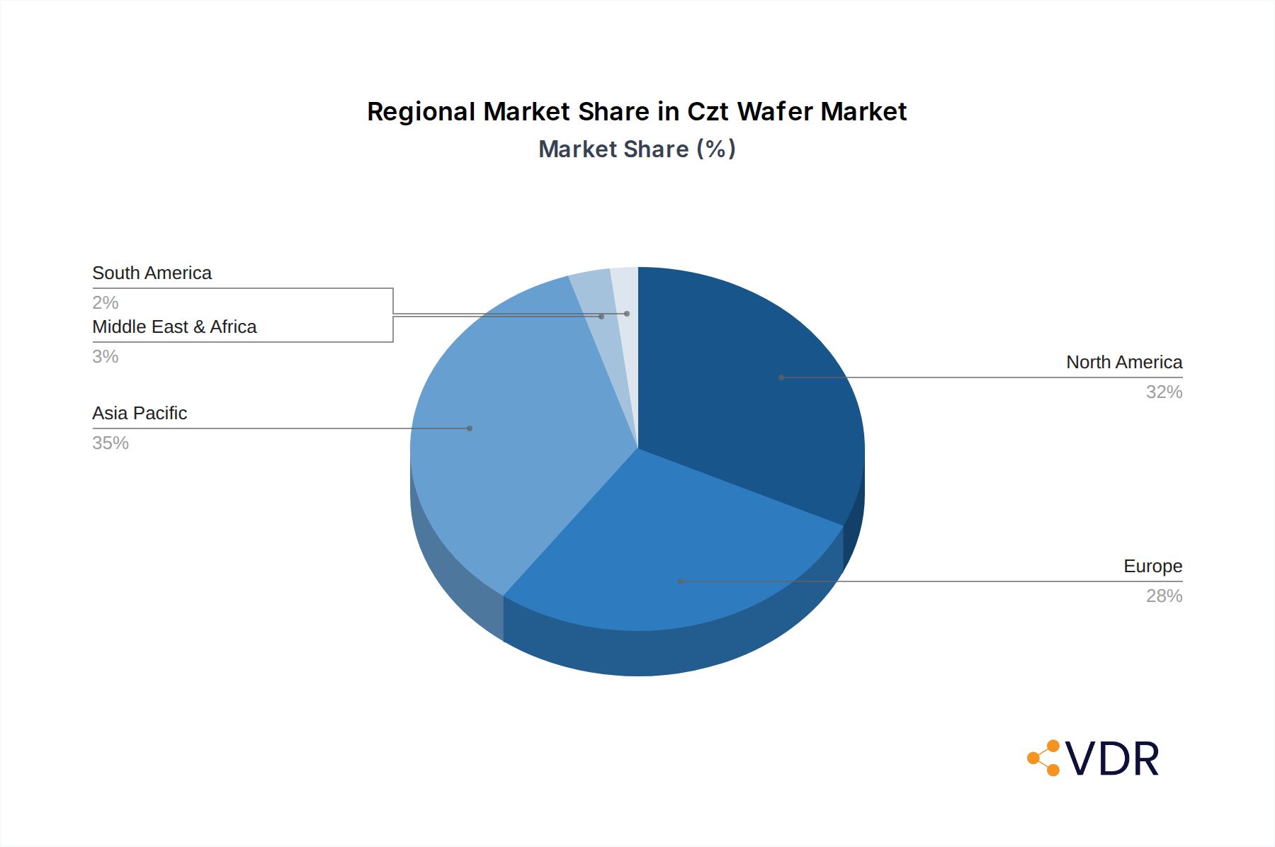
Czt Wafer Regional Market Share
Geographic Coverage of Czt Wafer
Czt Wafer REPORT HIGHLIGHTS
| Aspects | Details |
|---|---|
| Study Period | 2020-2034 |
| Base Year | 2025 |
| Estimated Year | 2026 |
| Forecast Period | 2026-2034 |
| Historical Period | 2020-2025 |
| Growth Rate | CAGR of 8.2% from 2020-2034 |
| Segmentation |
|
Table of Contents
- 1. Introduction
- 1.1. Research Scope
- 1.2. Market Segmentation
- 1.3. Research Objective
- 1.4. Definitions and Assumptions
- 2. Executive Summary
- 2.1. Market Snapshot
- 3. Market Dynamics
- 3.1. Market Drivers
- 3.2. Market Restrains
- 3.3. Market Trends
- 3.4. Market Opportunities
- 4. Market Factor Analysis
- 4.1. Porters Five Forces
- 4.1.1. Bargaining Power of Suppliers
- 4.1.2. Bargaining Power of Buyers
- 4.1.3. Threat of New Entrants
- 4.1.4. Threat of Substitutes
- 4.1.5. Competitive Rivalry
- 4.2. PESTEL analysis
- 4.3. BCG Analysis
- 4.3.1. Stars (High Growth, High Market Share)
- 4.3.2. Cash Cows (Low Growth, High Market Share)
- 4.3.3. Question Mark (High Growth, Low Market Share)
- 4.3.4. Dogs (Low Growth, Low Market Share)
- 4.4. Ansoff Matrix Analysis
- 4.5. Supply Chain Analysis
- 4.6. Regulatory Landscape
- 4.7. Current Market Potential and Opportunity Assessment (TAM–SAM–SOM Framework)
- 4.8. VDR Analyst Note
- 4.1. Porters Five Forces
- 5. Market Analysis, Insights and Forecast 2021-2033
- 5.1. Market Analysis, Insights and Forecast - by Application
- 5.1.1. Electronics & Semiconductors
- 5.1.2. Medical
- 5.1.3. Energy
- 5.1.4. Others
- 5.2. Market Analysis, Insights and Forecast - by Type
- 5.2.1. Single Crystal CZT Wafer
- 5.2.2. Polycrystalline CZT Wafer
- 5.2.3. Others
- 5.3. Market Analysis, Insights and Forecast - by Region
- 5.3.1. North America
- 5.3.2. South America
- 5.3.3. Europe
- 5.3.4. Middle East & Africa
- 5.3.5. Asia Pacific
- 5.1. Market Analysis, Insights and Forecast - by Application
- 6. Global Czt Wafer Analysis, Insights and Forecast, 2021-2033
- 6.1. Market Analysis, Insights and Forecast - by Application
- 6.1.1. Electronics & Semiconductors
- 6.1.2. Medical
- 6.1.3. Energy
- 6.1.4. Others
- 6.2. Market Analysis, Insights and Forecast - by Type
- 6.2.1. Single Crystal CZT Wafer
- 6.2.2. Polycrystalline CZT Wafer
- 6.2.3. Others
- 6.1. Market Analysis, Insights and Forecast - by Application
- 7. North America Czt Wafer Analysis, Insights and Forecast, 2021-2033
- 7.1. Market Analysis, Insights and Forecast - by Application
- 7.1.1. Electronics & Semiconductors
- 7.1.2. Medical
- 7.1.3. Energy
- 7.1.4. Others
- 7.2. Market Analysis, Insights and Forecast - by Type
- 7.2.1. Single Crystal CZT Wafer
- 7.2.2. Polycrystalline CZT Wafer
- 7.2.3. Others
- 7.1. Market Analysis, Insights and Forecast - by Application
- 8. South America Czt Wafer Analysis, Insights and Forecast, 2021-2033
- 8.1. Market Analysis, Insights and Forecast - by Application
- 8.1.1. Electronics & Semiconductors
- 8.1.2. Medical
- 8.1.3. Energy
- 8.1.4. Others
- 8.2. Market Analysis, Insights and Forecast - by Type
- 8.2.1. Single Crystal CZT Wafer
- 8.2.2. Polycrystalline CZT Wafer
- 8.2.3. Others
- 8.1. Market Analysis, Insights and Forecast - by Application
- 9. Europe Czt Wafer Analysis, Insights and Forecast, 2021-2033
- 9.1. Market Analysis, Insights and Forecast - by Application
- 9.1.1. Electronics & Semiconductors
- 9.1.2. Medical
- 9.1.3. Energy
- 9.1.4. Others
- 9.2. Market Analysis, Insights and Forecast - by Type
- 9.2.1. Single Crystal CZT Wafer
- 9.2.2. Polycrystalline CZT Wafer
- 9.2.3. Others
- 9.1. Market Analysis, Insights and Forecast - by Application
- 10. Middle East & Africa Czt Wafer Analysis, Insights and Forecast, 2021-2033
- 10.1. Market Analysis, Insights and Forecast - by Application
- 10.1.1. Electronics & Semiconductors
- 10.1.2. Medical
- 10.1.3. Energy
- 10.1.4. Others
- 10.2. Market Analysis, Insights and Forecast - by Type
- 10.2.1. Single Crystal CZT Wafer
- 10.2.2. Polycrystalline CZT Wafer
- 10.2.3. Others
- 10.1. Market Analysis, Insights and Forecast - by Application
- 11. Asia Pacific Czt Wafer Analysis, Insights and Forecast, 2021-2033
- 11.1. Market Analysis, Insights and Forecast - by Application
- 11.1.1. Electronics & Semiconductors
- 11.1.2. Medical
- 11.1.3. Energy
- 11.1.4. Others
- 11.2. Market Analysis, Insights and Forecast - by Type
- 11.2.1. Single Crystal CZT Wafer
- 11.2.2. Polycrystalline CZT Wafer
- 11.2.3. Others
- 11.1. Market Analysis, Insights and Forecast - by Application
- 12. Competitive Analysis
- 12.1. Company Profiles
- 12.1.1 Stanford Advanced Materials
- 12.1.1.1. Company Overview
- 12.1.1.2. Products
- 12.1.1.3. Company Financials
- 12.1.1.4. SWOT Analysis
- 12.1.2 MSE Supplies LLC
- 12.1.2.1. Company Overview
- 12.1.2.2. Products
- 12.1.2.3. Company Financials
- 12.1.2.4. SWOT Analysis
- 12.1.3 II-VI Incorporated
- 12.1.3.1. Company Overview
- 12.1.3.2. Products
- 12.1.3.3. Company Financials
- 12.1.3.4. SWOT Analysis
- 12.1.4 JX Nippon Mining & Metals Corporation
- 12.1.4.1. Company Overview
- 12.1.4.2. Products
- 12.1.4.3. Company Financials
- 12.1.4.4. SWOT Analysis
- 12.1.5 Shalom EO
- 12.1.5.1. Company Overview
- 12.1.5.2. Products
- 12.1.5.3. Company Financials
- 12.1.5.4. SWOT Analysis
- 12.1.6 Redlen Technologies Inc.
- 12.1.6.1. Company Overview
- 12.1.6.2. Products
- 12.1.6.3. Company Financials
- 12.1.6.4. SWOT Analysis
- 12.1.7 MTI Corporation
- 12.1.7.1. Company Overview
- 12.1.7.2. Products
- 12.1.7.3. Company Financials
- 12.1.7.4. SWOT Analysis
- 12.1.8 Ganwafer
- 12.1.8.1. Company Overview
- 12.1.8.2. Products
- 12.1.8.3. Company Financials
- 12.1.8.4. SWOT Analysis
- 12.1.9 PWAM
- 12.1.9.1. Company Overview
- 12.1.9.2. Products
- 12.1.9.3. Company Financials
- 12.1.9.4. SWOT Analysis
- 12.1.10 Kinheng Crystal
- 12.1.10.1. Company Overview
- 12.1.10.2. Products
- 12.1.10.3. Company Financials
- 12.1.10.4. SWOT Analysis
- 12.1.1 Stanford Advanced Materials
- 12.2. Market Entropy
- 12.2.1 Company's Key Areas Served
- 12.2.2 Recent Developments
- 12.3. Company Market Share Analysis 2025
- 12.3.1 Top 5 Companies Market Share Analysis
- 12.3.2 Top 3 Companies Market Share Analysis
- 12.4. List of Potential Customers
- 13. Research Methodology
List of Figures
- Figure 1: Global Czt Wafer Revenue Breakdown (million, %) by Region 2025 & 2033
- Figure 2: North America Czt Wafer Revenue (million), by Application 2025 & 2033
- Figure 3: North America Czt Wafer Revenue Share (%), by Application 2025 & 2033
- Figure 4: North America Czt Wafer Revenue (million), by Type 2025 & 2033
- Figure 5: North America Czt Wafer Revenue Share (%), by Type 2025 & 2033
- Figure 6: North America Czt Wafer Revenue (million), by Country 2025 & 2033
- Figure 7: North America Czt Wafer Revenue Share (%), by Country 2025 & 2033
- Figure 8: South America Czt Wafer Revenue (million), by Application 2025 & 2033
- Figure 9: South America Czt Wafer Revenue Share (%), by Application 2025 & 2033
- Figure 10: South America Czt Wafer Revenue (million), by Type 2025 & 2033
- Figure 11: South America Czt Wafer Revenue Share (%), by Type 2025 & 2033
- Figure 12: South America Czt Wafer Revenue (million), by Country 2025 & 2033
- Figure 13: South America Czt Wafer Revenue Share (%), by Country 2025 & 2033
- Figure 14: Europe Czt Wafer Revenue (million), by Application 2025 & 2033
- Figure 15: Europe Czt Wafer Revenue Share (%), by Application 2025 & 2033
- Figure 16: Europe Czt Wafer Revenue (million), by Type 2025 & 2033
- Figure 17: Europe Czt Wafer Revenue Share (%), by Type 2025 & 2033
- Figure 18: Europe Czt Wafer Revenue (million), by Country 2025 & 2033
- Figure 19: Europe Czt Wafer Revenue Share (%), by Country 2025 & 2033
- Figure 20: Middle East & Africa Czt Wafer Revenue (million), by Application 2025 & 2033
- Figure 21: Middle East & Africa Czt Wafer Revenue Share (%), by Application 2025 & 2033
- Figure 22: Middle East & Africa Czt Wafer Revenue (million), by Type 2025 & 2033
- Figure 23: Middle East & Africa Czt Wafer Revenue Share (%), by Type 2025 & 2033
- Figure 24: Middle East & Africa Czt Wafer Revenue (million), by Country 2025 & 2033
- Figure 25: Middle East & Africa Czt Wafer Revenue Share (%), by Country 2025 & 2033
- Figure 26: Asia Pacific Czt Wafer Revenue (million), by Application 2025 & 2033
- Figure 27: Asia Pacific Czt Wafer Revenue Share (%), by Application 2025 & 2033
- Figure 28: Asia Pacific Czt Wafer Revenue (million), by Type 2025 & 2033
- Figure 29: Asia Pacific Czt Wafer Revenue Share (%), by Type 2025 & 2033
- Figure 30: Asia Pacific Czt Wafer Revenue (million), by Country 2025 & 2033
- Figure 31: Asia Pacific Czt Wafer Revenue Share (%), by Country 2025 & 2033
List of Tables
- Table 1: Global Czt Wafer Revenue million Forecast, by Application 2020 & 2033
- Table 2: Global Czt Wafer Revenue million Forecast, by Type 2020 & 2033
- Table 3: Global Czt Wafer Revenue million Forecast, by Region 2020 & 2033
- Table 4: Global Czt Wafer Revenue million Forecast, by Application 2020 & 2033
- Table 5: Global Czt Wafer Revenue million Forecast, by Type 2020 & 2033
- Table 6: Global Czt Wafer Revenue million Forecast, by Country 2020 & 2033
- Table 7: United States Czt Wafer Revenue (million) Forecast, by Application 2020 & 2033
- Table 8: Canada Czt Wafer Revenue (million) Forecast, by Application 2020 & 2033
- Table 9: Mexico Czt Wafer Revenue (million) Forecast, by Application 2020 & 2033
- Table 10: Global Czt Wafer Revenue million Forecast, by Application 2020 & 2033
- Table 11: Global Czt Wafer Revenue million Forecast, by Type 2020 & 2033
- Table 12: Global Czt Wafer Revenue million Forecast, by Country 2020 & 2033
- Table 13: Brazil Czt Wafer Revenue (million) Forecast, by Application 2020 & 2033
- Table 14: Argentina Czt Wafer Revenue (million) Forecast, by Application 2020 & 2033
- Table 15: Rest of South America Czt Wafer Revenue (million) Forecast, by Application 2020 & 2033
- Table 16: Global Czt Wafer Revenue million Forecast, by Application 2020 & 2033
- Table 17: Global Czt Wafer Revenue million Forecast, by Type 2020 & 2033
- Table 18: Global Czt Wafer Revenue million Forecast, by Country 2020 & 2033
- Table 19: United Kingdom Czt Wafer Revenue (million) Forecast, by Application 2020 & 2033
- Table 20: Germany Czt Wafer Revenue (million) Forecast, by Application 2020 & 2033
- Table 21: France Czt Wafer Revenue (million) Forecast, by Application 2020 & 2033
- Table 22: Italy Czt Wafer Revenue (million) Forecast, by Application 2020 & 2033
- Table 23: Spain Czt Wafer Revenue (million) Forecast, by Application 2020 & 2033
- Table 24: Russia Czt Wafer Revenue (million) Forecast, by Application 2020 & 2033
- Table 25: Benelux Czt Wafer Revenue (million) Forecast, by Application 2020 & 2033
- Table 26: Nordics Czt Wafer Revenue (million) Forecast, by Application 2020 & 2033
- Table 27: Rest of Europe Czt Wafer Revenue (million) Forecast, by Application 2020 & 2033
- Table 28: Global Czt Wafer Revenue million Forecast, by Application 2020 & 2033
- Table 29: Global Czt Wafer Revenue million Forecast, by Type 2020 & 2033
- Table 30: Global Czt Wafer Revenue million Forecast, by Country 2020 & 2033
- Table 31: Turkey Czt Wafer Revenue (million) Forecast, by Application 2020 & 2033
- Table 32: Israel Czt Wafer Revenue (million) Forecast, by Application 2020 & 2033
- Table 33: GCC Czt Wafer Revenue (million) Forecast, by Application 2020 & 2033
- Table 34: North Africa Czt Wafer Revenue (million) Forecast, by Application 2020 & 2033
- Table 35: South Africa Czt Wafer Revenue (million) Forecast, by Application 2020 & 2033
- Table 36: Rest of Middle East & Africa Czt Wafer Revenue (million) Forecast, by Application 2020 & 2033
- Table 37: Global Czt Wafer Revenue million Forecast, by Application 2020 & 2033
- Table 38: Global Czt Wafer Revenue million Forecast, by Type 2020 & 2033
- Table 39: Global Czt Wafer Revenue million Forecast, by Country 2020 & 2033
- Table 40: China Czt Wafer Revenue (million) Forecast, by Application 2020 & 2033
- Table 41: India Czt Wafer Revenue (million) Forecast, by Application 2020 & 2033
- Table 42: Japan Czt Wafer Revenue (million) Forecast, by Application 2020 & 2033
- Table 43: South Korea Czt Wafer Revenue (million) Forecast, by Application 2020 & 2033
- Table 44: ASEAN Czt Wafer Revenue (million) Forecast, by Application 2020 & 2033
- Table 45: Oceania Czt Wafer Revenue (million) Forecast, by Application 2020 & 2033
- Table 46: Rest of Asia Pacific Czt Wafer Revenue (million) Forecast, by Application 2020 & 2033
Frequently Asked Questions
1. What is the projected Compound Annual Growth Rate (CAGR) of the Czt Wafer?
The projected CAGR is approximately 8.2%.
2. Which companies are prominent players in the Czt Wafer?
Key companies in the market include Stanford Advanced Materials, MSE Supplies LLC, II-VI Incorporated, JX Nippon Mining & Metals Corporation, Shalom EO, Redlen Technologies Inc., MTI Corporation, Ganwafer, PWAM, Kinheng Crystal.
3. What are the main segments of the Czt Wafer?
The market segments include Application, Type.
4. Can you provide details about the market size?
The market size is estimated to be USD 79.1 million as of 2022.
5. What are some drivers contributing to market growth?
N/A
6. What are the notable trends driving market growth?
N/A
7. Are there any restraints impacting market growth?
N/A
8. Can you provide examples of recent developments in the market?
N/A
9. What pricing options are available for accessing the report?
Pricing options include single-user, multi-user, and enterprise licenses priced at USD 4900.00, USD 7350.00, and USD 9800.00 respectively.
10. Is the market size provided in terms of value or volume?
The market size is provided in terms of value, measured in million.
11. Are there any specific market keywords associated with the report?
Yes, the market keyword associated with the report is "Czt Wafer," which aids in identifying and referencing the specific market segment covered.
12. How do I determine which pricing option suits my needs best?
The pricing options vary based on user requirements and access needs. Individual users may opt for single-user licenses, while businesses requiring broader access may choose multi-user or enterprise licenses for cost-effective access to the report.
13. Are there any additional resources or data provided in the Czt Wafer report?
While the report offers comprehensive insights, it's advisable to review the specific contents or supplementary materials provided to ascertain if additional resources or data are available.
14. How can I stay updated on further developments or reports in the Czt Wafer?
To stay informed about further developments, trends, and reports in the Czt Wafer, consider subscribing to industry newsletters, following relevant companies and organizations, or regularly checking reputable industry news sources and publications.
Methodology
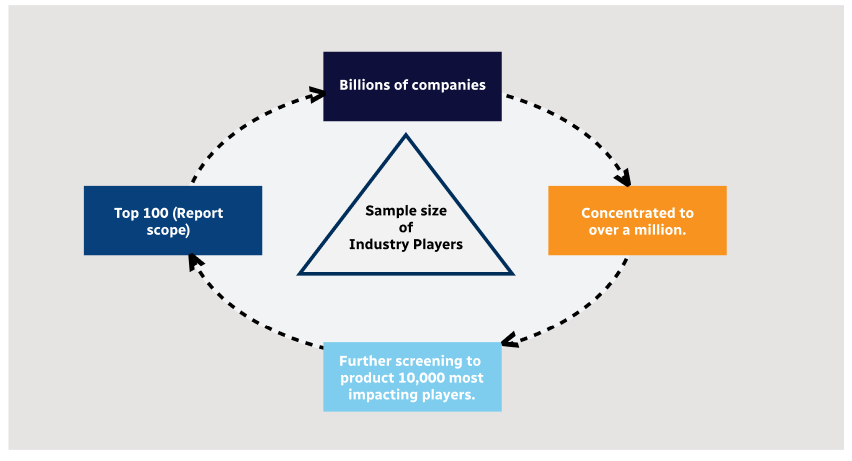
Step 1 - Identification of Relevant Samples Size from Population Database

Step 2 - Approaches for Defining Global Market Size (Value, Volume* & Price*)
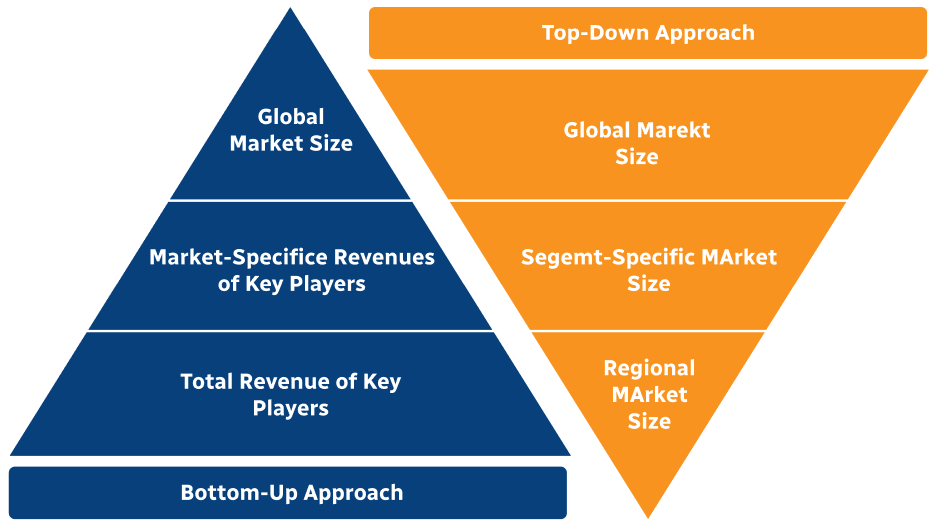
Note*: In applicable scenarios
Step 3 - Data Sources
Primary Research
- Web Analytics
- Survey Reports
- Research Institute
- Latest Research Reports
- Opinion Leaders
Secondary Research
- Annual Reports
- White Paper
- Latest Press Release
- Industry Association
- Paid Database
- Investor Presentations

Step 4 - Data Triangulation
Involves using different sources of information in order to increase the validity of a study
These sources are likely to be stakeholders in a program - participants, other researchers, program staff, other community members, and so on.
Then we put all data in single framework & apply various statistical tools to find out the dynamic on the market.
During the analysis stage, feedback from the stakeholder groups would be compared to determine areas of agreement as well as areas of divergence