

Key Insights
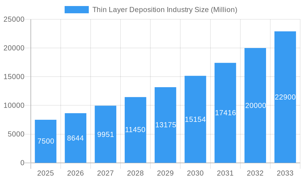
The global Thin Layer Deposition market is projected for significant growth, reaching $24.93 billion by 2025, with a projected Compound Annual Growth Rate (CAGR) of 14.78%. This expansion is driven by increasing demand in sectors such as advanced electronics, automotive (ADAS, EVs), medical devices, and renewable energy. Advancements in semiconductor technology and the miniaturization of components are fueling the adoption of deposition techniques like PVD, CVD, and ALD.
Thin Layer Deposition Industry Market Size (In Billion)
Key market trends include the growing application of ALD for its precision and the integration of thin-film technologies in IoT and wearable devices. While high capital investment and specialized expertise pose challenges, continuous innovation by leading players like Applied Materials, Tokyo Electron Limited, and ASM International NV is expected to drive market development. The Asia Pacific region, particularly China and South Korea, is anticipated to lead market share, supported by strong electronics manufacturing and rapid technological adoption. North America and Europe will also contribute significantly through innovations in automotive, medical, and energy applications.
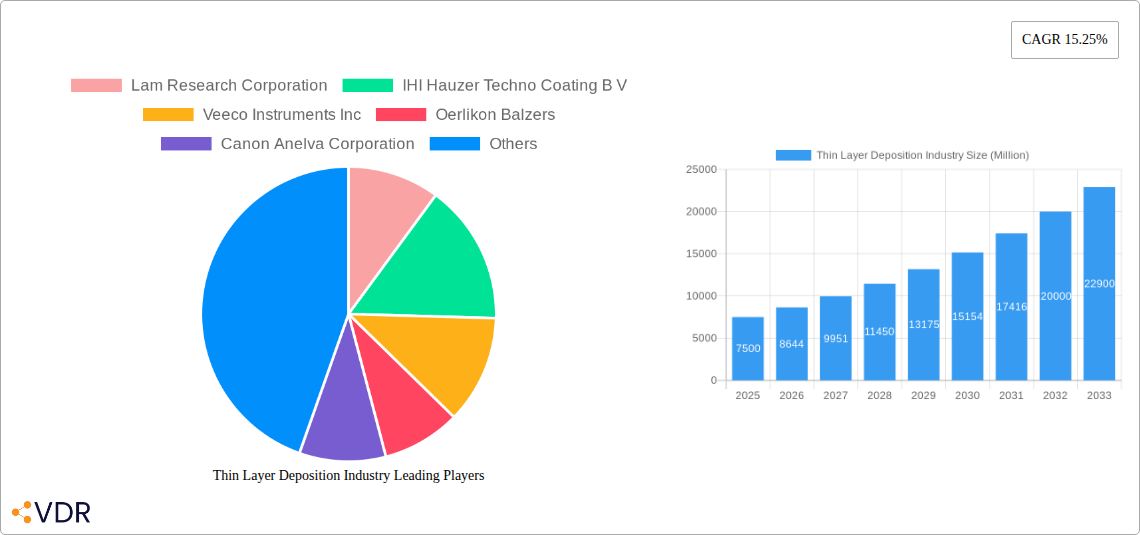
Thin Layer Deposition Industry Company Market Share
Thin Layer Deposition Industry Market Dynamics & Structure
The global thin layer deposition market is characterized by a moderately concentrated structure, with a few key players like Lam Research Corporation, Applied Materials Inc., and Tokyo Electron Limited holding significant market shares. This concentration is driven by high capital expenditure requirements for advanced equipment and extensive R&D investment necessary for continuous innovation. Technological innovation is the primary driver, fueled by the relentless demand for smaller, faster, and more efficient electronic devices. Advancements in Physical Vapor Deposition (PVD), particularly sputtering and evaporation techniques, alongside sophisticated Chemical Vapor Deposition (CVD) and the precision of Atomic Layer Deposition (ALD), are critical for fabricating next-generation semiconductors, advanced displays, and specialized coatings. Regulatory frameworks, primarily focused on environmental compliance and material safety, influence process development and material selection. Competitive product substitutes are limited within the core deposition technologies, but innovation in alternative manufacturing processes can pose a threat. End-user demographics are increasingly sophisticated, with the Electronics sector (including sub-segments like Automotive and Medical) exhibiting the strongest demand for advanced thin film solutions. Mergers and Acquisitions (M&A) trends, while not as frequent as in broader tech markets, are strategic, aiming to consolidate intellectual property, expand product portfolios, and gain access to new end-use industries. For instance, the acquisition of a niche ALD equipment provider by a larger player could significantly boost its market presence.
- Market Concentration: Top 5 players estimated to hold over 60% of the global market share.
- Technological Innovation Drivers: Miniaturization in electronics, demand for energy-efficient devices, development of novel materials (e.g., 2D materials, advanced dielectrics).
- Regulatory Frameworks: REACH compliance for materials, RoHS directives, environmental regulations on emissions from CVD processes.
- Competitive Product Substitutes: Emerging additive manufacturing techniques for certain coating applications, advanced material processing methods.
- End-User Demographics: Growing demand from automotive (ADAS, EVs), medical devices (sensors, implants), and renewable energy sectors.
- M&A Trends: Strategic acquisitions focusing on ALD expertise, specialized PVD/CVD coatings, and emerging market access.
Thin Layer Deposition Industry Growth Trends & Insights
The Thin Layer Deposition industry is poised for substantial growth, driven by its indispensable role in modern technological advancements. The global market size is projected to expand significantly from approximately USD 55,000 Million in 2023 to an estimated USD 85,000 Million by 2033, exhibiting a Compound Annual Growth Rate (CAGR) of 4.3% during the forecast period (2025-2033). This robust expansion is underpinned by escalating adoption rates of advanced semiconductor manufacturing techniques, particularly in the production of high-performance logic chips, memory devices, and cutting-edge display technologies. Technological disruptions are continuously reshaping the landscape, with ALD emerging as a critical technology for achieving atomic-level precision in film deposition, enabling the creation of ultra-thin, conformal layers essential for advanced logic nodes and 3D architectures. PVD technologies, including magnetron sputtering and ion beam deposition, remain vital for a wide array of applications, from protective coatings on optical lenses to conductive layers in displays. CVD, in its various forms like plasma-enhanced CVD (PECVD) and low-pressure CVD (LPCVD), continues to be a workhorse for depositing dielectric and semiconductor films. Consumer behavior shifts towards more sophisticated and interconnected devices, including wearables, advanced automotive electronics, and personalized medical equipment, are directly translating into increased demand for sophisticated thin film solutions. For instance, the growing demand for flexible OLED displays in smartphones and televisions is a significant market driver for specialized PVD and ALD processes. The automotive sector's transition to electric vehicles (EVs) and autonomous driving systems is creating unprecedented demand for advanced sensors, power electronics, and battery components, all of which rely heavily on precise thin layer deposition for enhanced performance and reliability. Furthermore, the burgeoning medical device industry, with its focus on miniaturization, biocompatibility, and advanced diagnostics, is increasingly turning to thin film coatings for implants, biosensors, and drug delivery systems. The energy sector, particularly in the development of solar cells and advanced battery technologies, also presents a significant growth avenue, where thin films play a crucial role in improving efficiency and durability. The increasing complexity of integrated circuits and the need for multi-layered structures in advanced packaging further fuel the demand for highly controlled deposition processes. This sustained innovation and broad application spectrum ensures a healthy growth trajectory for the thin layer deposition market throughout the forecast period. The market penetration of ALD is expected to witness a notable surge, driven by its unique capabilities in precise film control, essential for next-generation semiconductor nodes.
Dominant Regions, Countries, or Segments in Thin Layer Deposition Industry
The Thin Layer Deposition industry is currently dominated by the Electronics end-use industry segment, which accounts for a substantial portion of the global market revenue, estimated at over 70% in 2023. Within this segment, the burgeoning demand from the semiconductor manufacturing sector is the primary growth engine. The relentless pursuit of smaller, faster, and more energy-efficient chips for everything from smartphones and data centers to artificial intelligence and IoT devices necessitates advanced thin film deposition processes. Asia-Pacific, particularly Taiwan, South Korea, and China, stands out as the leading region, driven by the concentration of major semiconductor foundries and display manufacturers. These countries benefit from robust government support, significant investments in R&D, and a well-established ecosystem of component suppliers and research institutions.
Dominant End-Use Industry: Electronics
- Key Drivers:
- Semiconductor Manufacturing: Continuous innovation in logic and memory devices, advanced packaging technologies requiring precise multi-layer depositions. Market share for semiconductor applications is estimated to be around 65% of the total electronics segment.
- Display Technologies: Growth in OLED, micro-LED, and flexible display manufacturing, demanding specialized PVD and ALD for optical and conductive layers.
- Automotive Electronics: Increasing adoption of advanced driver-assistance systems (ADAS), in-car infotainment, and electric vehicle components, all requiring specialized sensors and power electronics with thin film coatings. Estimated growth for automotive applications is a CAGR of 5.5%.
- Medical Devices: Miniaturization of diagnostic tools, implantable devices, and biosensors driving demand for biocompatible and functional thin films.
- Market Share Analysis: The semiconductor segment within electronics alone represents an estimated USD 35,000 Million market in 2025.
- Key Drivers:
Dominant Deposition Technology: Physical Vapor Deposition (PVD)
- Key Drivers:
- Versatility and Cost-Effectiveness: PVD techniques like sputtering and evaporation are widely used for depositing a broad range of metallic, alloy, and dielectric films.
- High Throughput: PVD systems often offer higher throughput compared to some CVD processes, making them suitable for large-scale manufacturing.
- Applications: Widely used for conductive layers in semiconductors and displays, reflective coatings, and decorative finishes. Estimated market share of PVD in the total deposition technology market is 45%.
- Key Drivers:
Dominant Region: Asia-Pacific
- Key Drivers:
- Semiconductor Manufacturing Hubs: Concentration of leading foundries in Taiwan, South Korea, and China.
- Government Policies and Investments: Strong government support for the semiconductor and advanced manufacturing industries.
- Skilled Workforce and R&D Capabilities: Availability of a highly skilled technical workforce and robust research infrastructure.
- Growing Domestic Demand: Increasing consumer demand for electronics within the region.
- Country-Specific Dominance: Taiwan leads in foundry services, South Korea in memory and display manufacturing, and China is rapidly expanding its domestic semiconductor capacity.
- Key Drivers:
Growth Potential: While Electronics is dominant, the Automotive and Medical segments are exhibiting higher growth rates, indicating a future shift in market influence. The predicted CAGR for Automotive is 5.5% and for Medical is 6.2%. The growth of ALD is also projected to be a significant factor, with an estimated CAGR of 7.0%.
Thin Layer Deposition Industry Product Landscape
The product landscape of the thin layer deposition industry is characterized by continuous innovation and increasing sophistication. Key product developments focus on enhancing deposition precision, achieving higher throughput, and enabling the deposition of novel materials. Advanced PVD systems now incorporate sophisticated plasma control and substrate manipulation for improved film uniformity and adhesion. CVD equipment is evolving with enhanced gas delivery systems and reactor designs for greater control over film stoichiometry and morphology. Atomic Layer Deposition (ALD) systems are at the forefront of precision, enabling the deposition of ultra-thin, conformal films with atomic-level accuracy, critical for advanced semiconductor nodes and nanoscale devices. Innovations also include integrated multi-chamber systems that combine different deposition techniques and metrology tools for streamlined manufacturing workflows. Performance metrics such as film thickness uniformity (often within <1% variation), deposition rate, film purity, and conformal coverage are continuously being improved to meet the stringent demands of cutting-edge applications.
Key Drivers, Barriers & Challenges in Thin Layer Deposition Industry
Key Drivers:
The thin layer deposition industry is propelled by several key drivers. The relentless miniaturization and increasing complexity of electronic devices, particularly in the semiconductor sector, are paramount. Advancements in display technologies like OLED and micro-LED, alongside the growing demand for enhanced performance in automotive electronics and medical devices, further fuel innovation and adoption. The development of new materials with unique properties, such as 2D materials and advanced dielectrics, also necessitates sophisticated deposition techniques. Government initiatives promoting domestic manufacturing and R&D in advanced technologies also play a significant role.
Key Barriers & Challenges:
Despite its growth potential, the industry faces several challenges. High capital expenditure for advanced deposition equipment and the associated R&D costs present a significant barrier to entry for new players. The increasing stringency of environmental regulations related to process gases and waste management adds complexity and cost. Supply chain disruptions, particularly for specialized precursor materials and critical components, can impact production timelines and increase costs. Furthermore, the rapid pace of technological obsolescence requires continuous investment in upgrading equipment and expertise. The competitive pressure from alternative manufacturing processes and the need for highly skilled personnel to operate and maintain complex systems are also considerable challenges. For instance, a single advanced ALD tool can cost upwards of USD 5 Million.
Emerging Opportunities in Thin Layer Deposition Industry
Emerging opportunities lie in several high-growth areas. The expanding market for flexible electronics, driven by wearable devices and foldable displays, presents a significant avenue for specialized PVD and ALD applications. The rapid advancement of electric vehicles and autonomous driving technologies is creating demand for thin films in sensors, batteries, and power electronics. The medical sector's increasing reliance on advanced diagnostics and implantable devices, requiring biocompatible and functional thin film coatings, offers substantial growth potential. Furthermore, the development of next-generation energy storage solutions, including solid-state batteries and advanced solar cells, will heavily depend on novel thin layer deposition techniques. The adoption of AI and machine learning in optimizing deposition processes represents another significant emerging opportunity.
Growth Accelerators in the Thin Layer Deposition Industry Industry
Several catalysts are accelerating the long-term growth of the thin layer deposition industry. Technological breakthroughs, such as the development of novel precursor materials that enable lower deposition temperatures and higher purity films, are key accelerators. Strategic partnerships between equipment manufacturers and research institutions are fostering innovation and accelerating the commercialization of new technologies. Market expansion into emerging economies and new application areas, like advanced aerospace coatings and quantum computing components, will drive sustained growth. The increasing focus on energy efficiency and sustainability in manufacturing processes also presents an opportunity for deposition technologies that can reduce material waste and energy consumption. For example, breakthroughs in ALD for ultra-low-k dielectrics are essential for future chip advancements.
Key Players Shaping the Thin Layer Deposition Industry Market
- Lam Research Corporation
- IHI Hauzer Techno Coating B V
- Veeco Instruments Inc
- Oerlikon Balzers
- Canon Anelva Corporation
- CVD Equipment Corporation
- Applied Materials Inc
- ASM International NV
- Tokyo Electron Limited
- Aixtron SE
- Advanced Micro-Fabrication Equipment (AMEC)
Notable Milestones in Thin Layer Deposition Industry Sector
- 2019: Applied Materials introduces new PVD platform for advanced packaging, enhancing throughput and film quality.
- 2020: Veeco Instruments Inc. expands its ALD portfolio with new systems targeting advanced semiconductor nodes.
- 2021: Oerlikon Balzers acquires a specialist in surface solutions for the automotive sector, broadening its application reach.
- 2022: Tokyo Electron Limited (TEL) announces significant advancements in CVD technology for high-volume manufacturing of next-generation memory devices.
- 2023: Aixtron SE secures major orders for its advanced deposition tools from leading players in the compound semiconductor market.
- 2024: Canon Anelva Corporation releases a new generation of PVD equipment designed for increased efficiency and reduced environmental impact in display manufacturing.
In-Depth Thin Layer Deposition Industry Market Outlook
The outlook for the thin layer deposition industry is exceptionally strong, driven by continuous innovation and broad applicability across critical technology sectors. The market is expected to witness sustained growth propelled by advancements in AI, 5G, electric vehicles, and the burgeoning IoT ecosystem, all of which rely heavily on sophisticated semiconductor components manufactured using precise thin film deposition. Emerging opportunities in areas like advanced healthcare diagnostics, renewable energy storage, and potentially quantum computing will further diversify and expand the market. Strategic collaborations, R&D investments in novel materials and processes, and the expansion into new geographical markets will be key to capitalizing on this robust growth trajectory. The industry's ability to adapt to evolving environmental regulations and to develop more sustainable manufacturing solutions will also be crucial for long-term success. The market size is projected to reach USD 85,000 Million by 2033, indicating a significant expansion from its current USD 55,000 Million valuation.
Thin Layer Deposition Industry Segmentation
-
1. Deposition Technology
- 1.1. Physical Vapor Deposition (PVD)
- 1.2. Chemical Vapor Deposition (CVD)
- 1.3. Atomic Layer Deposition (ALD)
-
2. End-Use Industry
-
2.1. Electronics
-
2.1.1. Automotive
-
2.1.1.1. Medical
- 2.1.1.1.1. Energy
-
2.1.1.1. Medical
-
2.1.1. Automotive
-
2.1. Electronics
Thin Layer Deposition Industry Segmentation By Geography
- 1. North America: United States Canada Mexico
- 2. Europe: Germany: France: Italy: United Kingdom Netherlands Rest of Europe
- 3. Asia Pacific: China, Japan, India, South Korea, Taiwan, Australia, Rest of Asia-Pacific
- 4. South America : Brazil, Argentina, Rest of South America
- 5. MEA: Middle East, Africa
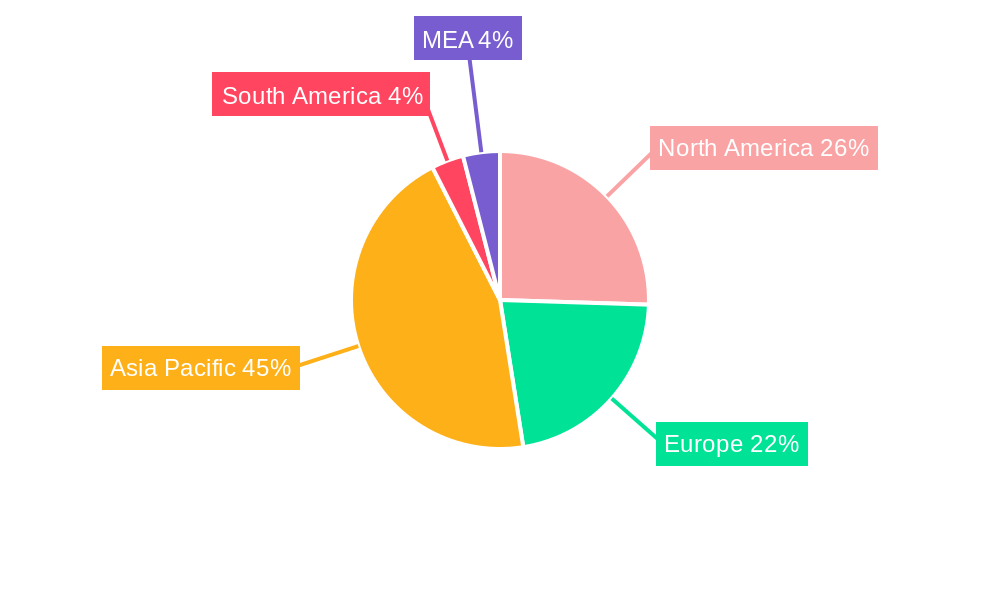
Thin Layer Deposition Industry Regional Market Share
Geographic Coverage of Thin Layer Deposition Industry
Thin Layer Deposition Industry REPORT HIGHLIGHTS
| Aspects | Details |
|---|---|
| Study Period | 2020-2034 |
| Base Year | 2025 |
| Estimated Year | 2026 |
| Forecast Period | 2026-2034 |
| Historical Period | 2020-2025 |
| Growth Rate | CAGR of 14.78% from 2020-2034 |
| Segmentation |
|
Table of Contents
- 1. Introduction
- 1.1. Research Scope
- 1.2. Market Segmentation
- 1.3. Research Objective
- 1.4. Definitions and Assumptions
- 2. Executive Summary
- 2.1. Market Snapshot
- 3. Market Dynamics
- 3.1. Market Drivers
- 3.2. Market Restrains
- 3.3. Market Trends
- 3.4. Market Opportunities
- 4. Market Factor Analysis
- 4.1. Porters Five Forces
- 4.1.1. Bargaining Power of Suppliers
- 4.1.2. Bargaining Power of Buyers
- 4.1.3. Threat of New Entrants
- 4.1.4. Threat of Substitutes
- 4.1.5. Competitive Rivalry
- 4.2. PESTEL analysis
- 4.3. BCG Analysis
- 4.3.1. Stars (High Growth, High Market Share)
- 4.3.2. Cash Cows (Low Growth, High Market Share)
- 4.3.3. Question Mark (High Growth, Low Market Share)
- 4.3.4. Dogs (Low Growth, Low Market Share)
- 4.4. Ansoff Matrix Analysis
- 4.5. Supply Chain Analysis
- 4.6. Regulatory Landscape
- 4.7. Current Market Potential and Opportunity Assessment (TAM–SAM–SOM Framework)
- 4.8. VDR Analyst Note
- 4.1. Porters Five Forces
- 5. Market Analysis, Insights and Forecast 2021-2033
- 5.1. Market Analysis, Insights and Forecast - by Deposition Technology
- 5.1.1. Physical Vapor Deposition (PVD)
- 5.1.2. Chemical Vapor Deposition (CVD)
- 5.1.3. Atomic Layer Deposition (ALD)
- 5.2. Market Analysis, Insights and Forecast - by End-Use Industry
- 5.2.1. Electronics
- 5.2.1.1. Automotive
- 5.2.1.1.1. Medical
- 5.2.1.1.1.1. Energy
- 5.2.1.1.1. Medical
- 5.2.1.1. Automotive
- 5.2.1. Electronics
- 5.3. Market Analysis, Insights and Forecast - by Region
- 5.3.1. North America: United States Canada Mexico
- 5.3.2. Europe: Germany: France: Italy: United Kingdom Netherlands Rest of Europe
- 5.3.3. Asia Pacific: China, Japan, India, South Korea, Taiwan, Australia, Rest of Asia-Pacific
- 5.3.4. South America : Brazil, Argentina, Rest of South America
- 5.3.5. MEA: Middle East, Africa
- 5.1. Market Analysis, Insights and Forecast - by Deposition Technology
- 6. Global Thin Layer Deposition Industry Analysis, Insights and Forecast, 2021-2033
- 6.1. Market Analysis, Insights and Forecast - by Deposition Technology
- 6.1.1. Physical Vapor Deposition (PVD)
- 6.1.2. Chemical Vapor Deposition (CVD)
- 6.1.3. Atomic Layer Deposition (ALD)
- 6.2. Market Analysis, Insights and Forecast - by End-Use Industry
- 6.2.1. Electronics
- 6.2.1.1. Automotive
- 6.2.1.1.1. Medical
- 6.2.1.1.1.1. Energy
- 6.2.1.1.1. Medical
- 6.2.1.1. Automotive
- 6.2.1. Electronics
- 6.1. Market Analysis, Insights and Forecast - by Deposition Technology
- 7. North America: United States Canada Mexico Thin Layer Deposition Industry Analysis, Insights and Forecast, 2021-2033
- 7.1. Market Analysis, Insights and Forecast - by Deposition Technology
- 7.1.1. Physical Vapor Deposition (PVD)
- 7.1.2. Chemical Vapor Deposition (CVD)
- 7.1.3. Atomic Layer Deposition (ALD)
- 7.2. Market Analysis, Insights and Forecast - by End-Use Industry
- 7.2.1. Electronics
- 7.2.1.1. Automotive
- 7.2.1.1.1. Medical
- 7.2.1.1.1.1. Energy
- 7.2.1.1.1. Medical
- 7.2.1.1. Automotive
- 7.2.1. Electronics
- 7.1. Market Analysis, Insights and Forecast - by Deposition Technology
- 8. Europe: Germany: France: Italy: United Kingdom Netherlands Rest of Europe Thin Layer Deposition Industry Analysis, Insights and Forecast, 2021-2033
- 8.1. Market Analysis, Insights and Forecast - by Deposition Technology
- 8.1.1. Physical Vapor Deposition (PVD)
- 8.1.2. Chemical Vapor Deposition (CVD)
- 8.1.3. Atomic Layer Deposition (ALD)
- 8.2. Market Analysis, Insights and Forecast - by End-Use Industry
- 8.2.1. Electronics
- 8.2.1.1. Automotive
- 8.2.1.1.1. Medical
- 8.2.1.1.1.1. Energy
- 8.2.1.1.1. Medical
- 8.2.1.1. Automotive
- 8.2.1. Electronics
- 8.1. Market Analysis, Insights and Forecast - by Deposition Technology
- 9. Asia Pacific: China, Japan, India, South Korea, Taiwan, Australia, Rest of Asia-Pacific Thin Layer Deposition Industry Analysis, Insights and Forecast, 2021-2033
- 9.1. Market Analysis, Insights and Forecast - by Deposition Technology
- 9.1.1. Physical Vapor Deposition (PVD)
- 9.1.2. Chemical Vapor Deposition (CVD)
- 9.1.3. Atomic Layer Deposition (ALD)
- 9.2. Market Analysis, Insights and Forecast - by End-Use Industry
- 9.2.1. Electronics
- 9.2.1.1. Automotive
- 9.2.1.1.1. Medical
- 9.2.1.1.1.1. Energy
- 9.2.1.1.1. Medical
- 9.2.1.1. Automotive
- 9.2.1. Electronics
- 9.1. Market Analysis, Insights and Forecast - by Deposition Technology
- 10. South America : Brazil, Argentina, Rest of South America Thin Layer Deposition Industry Analysis, Insights and Forecast, 2021-2033
- 10.1. Market Analysis, Insights and Forecast - by Deposition Technology
- 10.1.1. Physical Vapor Deposition (PVD)
- 10.1.2. Chemical Vapor Deposition (CVD)
- 10.1.3. Atomic Layer Deposition (ALD)
- 10.2. Market Analysis, Insights and Forecast - by End-Use Industry
- 10.2.1. Electronics
- 10.2.1.1. Automotive
- 10.2.1.1.1. Medical
- 10.2.1.1.1.1. Energy
- 10.2.1.1.1. Medical
- 10.2.1.1. Automotive
- 10.2.1. Electronics
- 10.1. Market Analysis, Insights and Forecast - by Deposition Technology
- 11. MEA: Middle East, Africa Thin Layer Deposition Industry Analysis, Insights and Forecast, 2021-2033
- 11.1. Market Analysis, Insights and Forecast - by Deposition Technology
- 11.1.1. Physical Vapor Deposition (PVD)
- 11.1.2. Chemical Vapor Deposition (CVD)
- 11.1.3. Atomic Layer Deposition (ALD)
- 11.2. Market Analysis, Insights and Forecast - by End-Use Industry
- 11.2.1. Electronics
- 11.2.1.1. Automotive
- 11.2.1.1.1. Medical
- 11.2.1.1.1.1. Energy
- 11.2.1.1.1. Medical
- 11.2.1.1. Automotive
- 11.2.1. Electronics
- 11.1. Market Analysis, Insights and Forecast - by Deposition Technology
- 12. Competitive Analysis
- 12.1. Company Profiles
- 12.1.1 Lam Research Corporation
- 12.1.1.1. Company Overview
- 12.1.1.2. Products
- 12.1.1.3. Company Financials
- 12.1.1.4. SWOT Analysis
- 12.1.2 IHI Hauzer Techno Coating B V
- 12.1.2.1. Company Overview
- 12.1.2.2. Products
- 12.1.2.3. Company Financials
- 12.1.2.4. SWOT Analysis
- 12.1.3 Veeco Instruments Inc
- 12.1.3.1. Company Overview
- 12.1.3.2. Products
- 12.1.3.3. Company Financials
- 12.1.3.4. SWOT Analysis
- 12.1.4 Oerlikon Balzers
- 12.1.4.1. Company Overview
- 12.1.4.2. Products
- 12.1.4.3. Company Financials
- 12.1.4.4. SWOT Analysis
- 12.1.5 Canon Anelva Corporation
- 12.1.5.1. Company Overview
- 12.1.5.2. Products
- 12.1.5.3. Company Financials
- 12.1.5.4. SWOT Analysis
- 12.1.6 CVD Equipment Corporation
- 12.1.6.1. Company Overview
- 12.1.6.2. Products
- 12.1.6.3. Company Financials
- 12.1.6.4. SWOT Analysis
- 12.1.7 Applied Materials Inc
- 12.1.7.1. Company Overview
- 12.1.7.2. Products
- 12.1.7.3. Company Financials
- 12.1.7.4. SWOT Analysis
- 12.1.8 ASM International NV
- 12.1.8.1. Company Overview
- 12.1.8.2. Products
- 12.1.8.3. Company Financials
- 12.1.8.4. SWOT Analysis
- 12.1.9 Tokyo Electron Limited
- 12.1.9.1. Company Overview
- 12.1.9.2. Products
- 12.1.9.3. Company Financials
- 12.1.9.4. SWOT Analysis
- 12.1.10 Aixtron SE
- 12.1.10.1. Company Overview
- 12.1.10.2. Products
- 12.1.10.3. Company Financials
- 12.1.10.4. SWOT Analysis
- 12.1.11 Advanced Micro-Fabrication Equipment (AMEC)
- 12.1.11.1. Company Overview
- 12.1.11.2. Products
- 12.1.11.3. Company Financials
- 12.1.11.4. SWOT Analysis
- 12.1.1 Lam Research Corporation
- 12.2. Market Entropy
- 12.2.1 Company's Key Areas Served
- 12.2.2 Recent Developments
- 12.3. Company Market Share Analysis 2025
- 12.3.1 Top 5 Companies Market Share Analysis
- 12.3.2 Top 3 Companies Market Share Analysis
- 12.4. List of Potential Customers
- 13. Research Methodology
List of Figures
- Figure 1: Global Thin Layer Deposition Industry Revenue Breakdown (billion, %) by Region 2025 & 2033
- Figure 2: North America: United States Canada Mexico Thin Layer Deposition Industry Revenue (billion), by Deposition Technology 2025 & 2033
- Figure 3: North America: United States Canada Mexico Thin Layer Deposition Industry Revenue Share (%), by Deposition Technology 2025 & 2033
- Figure 4: North America: United States Canada Mexico Thin Layer Deposition Industry Revenue (billion), by End-Use Industry 2025 & 2033
- Figure 5: North America: United States Canada Mexico Thin Layer Deposition Industry Revenue Share (%), by End-Use Industry 2025 & 2033
- Figure 6: North America: United States Canada Mexico Thin Layer Deposition Industry Revenue (billion), by Country 2025 & 2033
- Figure 7: North America: United States Canada Mexico Thin Layer Deposition Industry Revenue Share (%), by Country 2025 & 2033
- Figure 8: Europe: Germany: France: Italy: United Kingdom Netherlands Rest of Europe Thin Layer Deposition Industry Revenue (billion), by Deposition Technology 2025 & 2033
- Figure 9: Europe: Germany: France: Italy: United Kingdom Netherlands Rest of Europe Thin Layer Deposition Industry Revenue Share (%), by Deposition Technology 2025 & 2033
- Figure 10: Europe: Germany: France: Italy: United Kingdom Netherlands Rest of Europe Thin Layer Deposition Industry Revenue (billion), by End-Use Industry 2025 & 2033
- Figure 11: Europe: Germany: France: Italy: United Kingdom Netherlands Rest of Europe Thin Layer Deposition Industry Revenue Share (%), by End-Use Industry 2025 & 2033
- Figure 12: Europe: Germany: France: Italy: United Kingdom Netherlands Rest of Europe Thin Layer Deposition Industry Revenue (billion), by Country 2025 & 2033
- Figure 13: Europe: Germany: France: Italy: United Kingdom Netherlands Rest of Europe Thin Layer Deposition Industry Revenue Share (%), by Country 2025 & 2033
- Figure 14: Asia Pacific: China, Japan, India, South Korea, Taiwan, Australia, Rest of Asia-Pacific Thin Layer Deposition Industry Revenue (billion), by Deposition Technology 2025 & 2033
- Figure 15: Asia Pacific: China, Japan, India, South Korea, Taiwan, Australia, Rest of Asia-Pacific Thin Layer Deposition Industry Revenue Share (%), by Deposition Technology 2025 & 2033
- Figure 16: Asia Pacific: China, Japan, India, South Korea, Taiwan, Australia, Rest of Asia-Pacific Thin Layer Deposition Industry Revenue (billion), by End-Use Industry 2025 & 2033
- Figure 17: Asia Pacific: China, Japan, India, South Korea, Taiwan, Australia, Rest of Asia-Pacific Thin Layer Deposition Industry Revenue Share (%), by End-Use Industry 2025 & 2033
- Figure 18: Asia Pacific: China, Japan, India, South Korea, Taiwan, Australia, Rest of Asia-Pacific Thin Layer Deposition Industry Revenue (billion), by Country 2025 & 2033
- Figure 19: Asia Pacific: China, Japan, India, South Korea, Taiwan, Australia, Rest of Asia-Pacific Thin Layer Deposition Industry Revenue Share (%), by Country 2025 & 2033
- Figure 20: South America : Brazil, Argentina, Rest of South America Thin Layer Deposition Industry Revenue (billion), by Deposition Technology 2025 & 2033
- Figure 21: South America : Brazil, Argentina, Rest of South America Thin Layer Deposition Industry Revenue Share (%), by Deposition Technology 2025 & 2033
- Figure 22: South America : Brazil, Argentina, Rest of South America Thin Layer Deposition Industry Revenue (billion), by End-Use Industry 2025 & 2033
- Figure 23: South America : Brazil, Argentina, Rest of South America Thin Layer Deposition Industry Revenue Share (%), by End-Use Industry 2025 & 2033
- Figure 24: South America : Brazil, Argentina, Rest of South America Thin Layer Deposition Industry Revenue (billion), by Country 2025 & 2033
- Figure 25: South America : Brazil, Argentina, Rest of South America Thin Layer Deposition Industry Revenue Share (%), by Country 2025 & 2033
- Figure 26: MEA: Middle East, Africa Thin Layer Deposition Industry Revenue (billion), by Deposition Technology 2025 & 2033
- Figure 27: MEA: Middle East, Africa Thin Layer Deposition Industry Revenue Share (%), by Deposition Technology 2025 & 2033
- Figure 28: MEA: Middle East, Africa Thin Layer Deposition Industry Revenue (billion), by End-Use Industry 2025 & 2033
- Figure 29: MEA: Middle East, Africa Thin Layer Deposition Industry Revenue Share (%), by End-Use Industry 2025 & 2033
- Figure 30: MEA: Middle East, Africa Thin Layer Deposition Industry Revenue (billion), by Country 2025 & 2033
- Figure 31: MEA: Middle East, Africa Thin Layer Deposition Industry Revenue Share (%), by Country 2025 & 2033
List of Tables
- Table 1: Global Thin Layer Deposition Industry Revenue billion Forecast, by Deposition Technology 2020 & 2033
- Table 2: Global Thin Layer Deposition Industry Revenue billion Forecast, by End-Use Industry 2020 & 2033
- Table 3: Global Thin Layer Deposition Industry Revenue billion Forecast, by Region 2020 & 2033
- Table 4: Global Thin Layer Deposition Industry Revenue billion Forecast, by Deposition Technology 2020 & 2033
- Table 5: Global Thin Layer Deposition Industry Revenue billion Forecast, by End-Use Industry 2020 & 2033
- Table 6: Global Thin Layer Deposition Industry Revenue billion Forecast, by Country 2020 & 2033
- Table 7: Global Thin Layer Deposition Industry Revenue billion Forecast, by Deposition Technology 2020 & 2033
- Table 8: Global Thin Layer Deposition Industry Revenue billion Forecast, by End-Use Industry 2020 & 2033
- Table 9: Global Thin Layer Deposition Industry Revenue billion Forecast, by Country 2020 & 2033
- Table 10: Global Thin Layer Deposition Industry Revenue billion Forecast, by Deposition Technology 2020 & 2033
- Table 11: Global Thin Layer Deposition Industry Revenue billion Forecast, by End-Use Industry 2020 & 2033
- Table 12: Global Thin Layer Deposition Industry Revenue billion Forecast, by Country 2020 & 2033
- Table 13: Global Thin Layer Deposition Industry Revenue billion Forecast, by Deposition Technology 2020 & 2033
- Table 14: Global Thin Layer Deposition Industry Revenue billion Forecast, by End-Use Industry 2020 & 2033
- Table 15: Global Thin Layer Deposition Industry Revenue billion Forecast, by Country 2020 & 2033
- Table 16: Global Thin Layer Deposition Industry Revenue billion Forecast, by Deposition Technology 2020 & 2033
- Table 17: Global Thin Layer Deposition Industry Revenue billion Forecast, by End-Use Industry 2020 & 2033
- Table 18: Global Thin Layer Deposition Industry Revenue billion Forecast, by Country 2020 & 2033
Frequently Asked Questions
1. What is the projected Compound Annual Growth Rate (CAGR) of the Thin Layer Deposition Industry?
The projected CAGR is approximately 14.78%.
2. Which companies are prominent players in the Thin Layer Deposition Industry?
Key companies in the market include Lam Research Corporation, IHI Hauzer Techno Coating B V, Veeco Instruments Inc, Oerlikon Balzers, Canon Anelva Corporation, CVD Equipment Corporation, Applied Materials Inc, ASM International NV, Tokyo Electron Limited, Aixtron SE, Advanced Micro-Fabrication Equipment (AMEC).
3. What are the main segments of the Thin Layer Deposition Industry?
The market segments include Deposition Technology, End-Use Industry.
4. Can you provide details about the market size?
The market size is estimated to be USD 24.93 billion as of 2022.
5. What are some drivers contributing to market growth?
; Increase in Demand for Microelectronics and Consumer Electronics to Fuel the Demand; Surge in Demand of Sensors in the Smartphone Industry and Increasing Application of Solar Systems.
6. What are the notable trends driving market growth?
Increase in Demand for Microelectronics and Consumer Electronics to Fuel the Demand.
7. Are there any restraints impacting market growth?
; High Set up Cost; Increasing Cost of Raw Material.
8. Can you provide examples of recent developments in the market?
N/A
9. What pricing options are available for accessing the report?
Pricing options include single-user, multi-user, and enterprise licenses priced at USD 4750, USD 5250, and USD 8750 respectively.
10. Is the market size provided in terms of value or volume?
The market size is provided in terms of value, measured in billion.
11. Are there any specific market keywords associated with the report?
Yes, the market keyword associated with the report is "Thin Layer Deposition Industry," which aids in identifying and referencing the specific market segment covered.
12. How do I determine which pricing option suits my needs best?
The pricing options vary based on user requirements and access needs. Individual users may opt for single-user licenses, while businesses requiring broader access may choose multi-user or enterprise licenses for cost-effective access to the report.
13. Are there any additional resources or data provided in the Thin Layer Deposition Industry report?
While the report offers comprehensive insights, it's advisable to review the specific contents or supplementary materials provided to ascertain if additional resources or data are available.
14. How can I stay updated on further developments or reports in the Thin Layer Deposition Industry?
To stay informed about further developments, trends, and reports in the Thin Layer Deposition Industry, consider subscribing to industry newsletters, following relevant companies and organizations, or regularly checking reputable industry news sources and publications.
Methodology
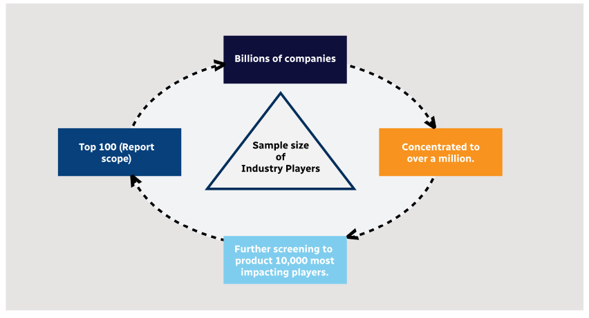
Step 1 - Identification of Relevant Samples Size from Population Database

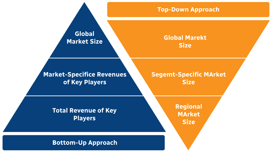
Step 2 - Approaches for Defining Global Market Size (Value, Volume* & Price*)
Note*: In applicable scenarios
Step 3 - Data Sources
Primary Research
- Web Analytics
- Survey Reports
- Research Institute
- Latest Research Reports
- Opinion Leaders
Secondary Research
- Annual Reports
- White Paper
- Latest Press Release
- Industry Association
- Paid Database
- Investor Presentations

Step 4 - Data Triangulation
Involves using different sources of information in order to increase the validity of a study
These sources are likely to be stakeholders in a program - participants, other researchers, program staff, other community members, and so on.
Then we put all data in single framework & apply various statistical tools to find out the dynamic on the market.
During the analysis stage, feedback from the stakeholder groups would be compared to determine areas of agreement as well as areas of divergence