


Key Insights
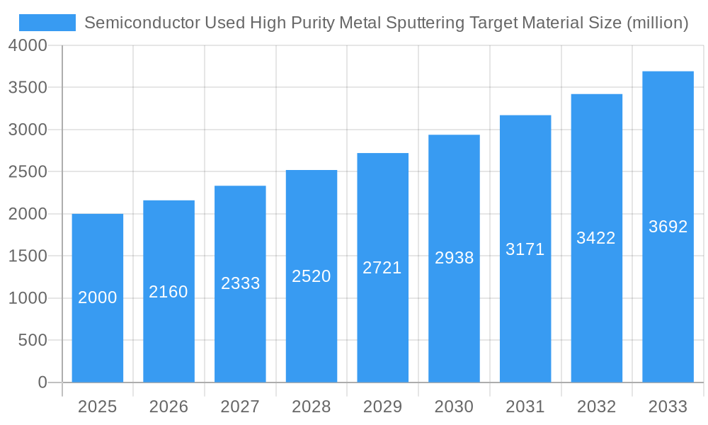
The semiconductor industry's drive for enhanced performance and miniaturization fuels significant demand for high-purity metal sputtering targets. This market, valued at $2.09 billion in 2025, is projected to grow at a compound annual growth rate (CAGR) of 4.2% from 2025 to 2033. This expansion is propelled by the increasing adoption of advanced semiconductor manufacturing nodes, essential for producing logic and memory devices that require highly precise and pure target materials for optimal thin-film deposition. Key growth drivers include the rising demand for 3D NAND flash memory, the expansion of 5G infrastructure, and the burgeoning automotive semiconductor sector. Challenges such as high raw material costs, stringent purity standards, and complex manufacturing processes persist. Leading companies are investing in research and development to overcome these hurdles and capitalize on market growth. The market is segmented by material type (aluminum, copper, titanium, tantalum), application (logic chips, memory, sensors), and region, with Asia-Pacific anticipated to dominate due to its concentration of semiconductor manufacturing.
Semiconductor Used High Purity Metal Sputtering Target Material Market Size (In Billion)

The competitive environment features established and emerging players focused on material purity, advanced manufacturing, and customer relationships. Innovation in developing next-generation materials with enhanced properties is a key trend, alongside a growing emphasis on sustainable and environmentally friendly manufacturing processes. This continuous innovation and consistent demand from the semiconductor sector will ensure the sustained growth of the high-purity metal sputtering target material market.
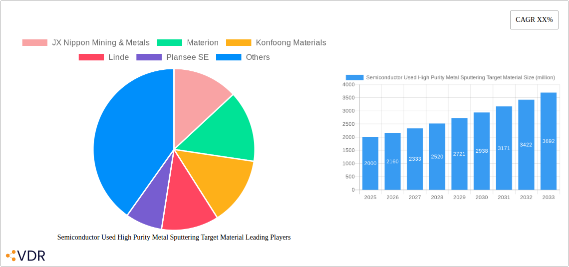
Semiconductor Used High Purity Metal Sputtering Target Material Company Market Share
Semiconductor Used High Purity Metal Sputtering Target Material Market Report: 2019-2033
This comprehensive report provides an in-depth analysis of the semiconductor used high-purity metal sputtering target material market, encompassing market dynamics, growth trends, regional dominance, product landscape, key players, and future outlook. The study period covers 2019-2033, with a base year of 2025 and a forecast period of 2025-2033. The report is crucial for semiconductor manufacturers, material suppliers, investors, and industry professionals seeking to understand this dynamic and rapidly evolving market. The parent market is the semiconductor industry (valued at xx million units in 2025), and the child market is high-purity metal sputtering target materials.
Semiconductor Used High Purity Metal Sputtering Target Material Market Dynamics & Structure
The semiconductor used high-purity metal sputtering target material market is characterized by moderate concentration, with several key players holding significant market share. Technological innovation, driven by the demand for advanced semiconductor devices, is a primary growth driver. Stringent regulatory frameworks concerning material purity and environmental impact influence market dynamics. Competitive product substitutes, such as pulsed laser deposition (PLD) techniques, exert pressure on market growth. The end-user demographics are predominantly semiconductor manufacturers across various segments, including memory, logic, and analog integrated circuits. M&A activity has been relatively moderate in recent years, with xx major deals recorded between 2019 and 2024, representing a total value of xx million units.
- Market Concentration: Moderately concentrated, with top 5 players holding approximately xx% market share in 2025.
- Technological Innovation: Focus on developing targets with enhanced purity, improved deposition rates, and reduced defect density.
- Regulatory Framework: Compliance with RoHS, REACH, and other environmental regulations is crucial.
- Competitive Substitutes: Pulsed laser deposition (PLD) and other thin-film deposition techniques pose a competitive threat.
- End-User Demographics: Primarily semiconductor manufacturers across various application segments.
- M&A Trends: Consolidation through mergers and acquisitions is expected to increase slightly in the coming years.
Semiconductor Used High Purity Metal Sputtering Target Material Growth Trends & Insights
The global semiconductor used high-purity metal sputtering target material market is experiencing robust growth, fueled by the increasing demand for advanced semiconductor devices in electronics, automotive, and industrial applications. The market size, valued at xx million units in 2025, is projected to reach xx million units by 2033, exhibiting a CAGR of xx% during the forecast period. This growth is driven by several factors, including the rising adoption of advanced semiconductor technologies like 5G, AI, and IoT. Technological disruptions, such as the development of new sputtering techniques and materials, further contribute to market expansion. Consumer behavior shifts towards high-performance electronic devices also support market growth. Market penetration in emerging economies is gradually increasing.
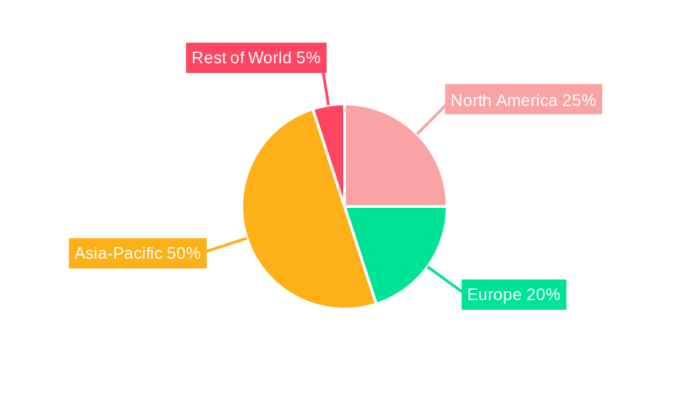
Dominant Regions, Countries, or Segments in Semiconductor Used High Purity Metal Sputtering Target Material
East Asia, particularly China, South Korea, and Taiwan, dominates the semiconductor used high-purity metal sputtering target material market, accounting for xx% of the global market share in 2025. This dominance is primarily attributed to the concentration of major semiconductor manufacturing facilities and robust government support for the semiconductor industry. North America and Europe also hold significant market shares, driven by established semiconductor industries and technological advancements. The memory segment is the largest consumer of high-purity metal sputtering targets, owing to high volume production.
- East Asia: High concentration of semiconductor manufacturing facilities and strong government support.
- North America: Strong presence of established semiconductor companies and ongoing technological innovations.
- Europe: Focus on specialized applications and high-value semiconductor manufacturing.
- Memory Segment: Highest volume consumption due to high demand for memory chips.
Semiconductor Used High Purity Metal Sputtering Target Material Product Landscape
The product landscape comprises a wide range of high-purity metals, including aluminum, copper, titanium, tantalum, and others, tailored for specific semiconductor applications. Continuous advancements focus on improving target purity, enhancing deposition rates, and reducing defects in the deposited films. Unique selling propositions include enhanced material properties, improved process efficiency, and minimized environmental impact. Technological advancements center around novel materials, improved manufacturing processes, and customized target designs to meet specific application needs.
Key Drivers, Barriers & Challenges in Semiconductor Used High Purity Metal Sputtering Target Material
Key Drivers:
- Increasing demand for advanced semiconductor devices driven by technological advancements in 5G, AI, IoT, and electric vehicles.
- Growing investments in semiconductor manufacturing capacity globally.
- Development of new sputtering techniques for improved deposition quality and efficiency.
Challenges & Restraints:
- Fluctuations in raw material prices and supply chain disruptions can impact production costs and profitability.
- Stringent environmental regulations pose challenges for manufacturers.
- Intense competition among established players and new entrants.
Emerging Opportunities in Semiconductor Used High Purity Metal Sputtering Target Material
- Growth in the power electronics and automotive semiconductor segments offers lucrative opportunities.
- Development of novel sputtering target materials with enhanced performance characteristics.
- Exploration of new applications in emerging technologies like quantum computing and flexible electronics.
Growth Accelerators in the Semiconductor Used High Purity Metal Sputtering Target Material Industry
Technological breakthroughs in sputtering technology, along with strategic partnerships between material suppliers and semiconductor manufacturers, are key catalysts for long-term growth. Market expansion into emerging economies and diversification into new applications further accelerate market growth.
Key Players Shaping the Semiconductor Used High Purity Metal Sputtering Target Material Market
- JX Nippon Mining & Metals
- Materion
- Konfoong Materials
- Linde
- Plansee SE
- Honeywell
- TOSOH
- TANAKA
- ULVAC
- Luvata
- Hitachi Metals
- Sumitomo Chemical
- Longhua Technology Group (Luoyang)
- GRIKIN Advanced Material
- Umicore
- Angstrom Sciences
- Advantec
- Changzhou Sujing Electronic Material
Notable Milestones in Semiconductor Used High Purity Metal Sputtering Target Material Sector
- 2021: Introduction of a new high-purity aluminum sputtering target with improved deposition rate by Materion.
- 2022: JX Nippon Mining & Metals announced a strategic partnership with a major semiconductor manufacturer for the supply of specialized sputtering targets.
- 2023: Several companies invested heavily in expanding their sputtering target manufacturing capabilities.
In-Depth Semiconductor Used High Purity Metal Sputtering Target Material Market Outlook
The semiconductor used high-purity metal sputtering target material market is poised for sustained growth, driven by the ongoing expansion of the semiconductor industry and technological advancements. Strategic partnerships, investments in R&D, and the development of innovative materials will continue to shape market dynamics. The market presents significant opportunities for both established players and new entrants with a focus on innovation and technological leadership.
Semiconductor Used High Purity Metal Sputtering Target Material Segmentation
-
1. Application
- 1.1. Consumer Electronics
- 1.2. Vehicle Electronics
- 1.3. Communication Electronics
- 1.4. Others
-
2. Types
- 2.1. Aluminum Target
- 2.2. Titanium Target
- 2.3. Tantalum Target
- 2.4. Copper Target
- 2.5. Others
Semiconductor Used High Purity Metal Sputtering Target Material Segmentation By Geography
-
1. North America
- 1.1. United States
- 1.2. Canada
- 1.3. Mexico
-
2. South America
- 2.1. Brazil
- 2.2. Argentina
- 2.3. Rest of South America
-
3. Europe
- 3.1. United Kingdom
- 3.2. Germany
- 3.3. France
- 3.4. Italy
- 3.5. Spain
- 3.6. Russia
- 3.7. Benelux
- 3.8. Nordics
- 3.9. Rest of Europe
-
4. Middle East & Africa
- 4.1. Turkey
- 4.2. Israel
- 4.3. GCC
- 4.4. North Africa
- 4.5. South Africa
- 4.6. Rest of Middle East & Africa
-
5. Asia Pacific
- 5.1. China
- 5.2. India
- 5.3. Japan
- 5.4. South Korea
- 5.5. ASEAN
- 5.6. Oceania
- 5.7. Rest of Asia Pacific
Semiconductor Used High Purity Metal Sputtering Target Material Regional Market Share
Geographic Coverage of Semiconductor Used High Purity Metal Sputtering Target Material
Semiconductor Used High Purity Metal Sputtering Target Material REPORT HIGHLIGHTS
| Aspects | Details |
|---|---|
| Study Period | 2020-2034 |
| Base Year | 2025 |
| Estimated Year | 2026 |
| Forecast Period | 2026-2034 |
| Historical Period | 2020-2025 |
| Growth Rate | CAGR of 4.2% from 2020-2034 |
| Segmentation |
|
Table of Contents
- 1. Introduction
- 1.1. Research Scope
- 1.2. Market Segmentation
- 1.3. Research Methodology
- 1.4. Definitions and Assumptions
- 2. Executive Summary
- 2.1. Introduction
- 3. Market Dynamics
- 3.1. Introduction
- 3.2. Market Drivers
- 3.3. Market Restrains
- 3.4. Market Trends
- 4. Market Factor Analysis
- 4.1. Porters Five Forces
- 4.2. Supply/Value Chain
- 4.3. PESTEL analysis
- 4.4. Market Entropy
- 4.5. Patent/Trademark Analysis
- 5. Global Semiconductor Used High Purity Metal Sputtering Target Material Analysis, Insights and Forecast, 2020-2032
- 5.1. Market Analysis, Insights and Forecast - by Application
- 5.1.1. Consumer Electronics
- 5.1.2. Vehicle Electronics
- 5.1.3. Communication Electronics
- 5.1.4. Others
- 5.2. Market Analysis, Insights and Forecast - by Types
- 5.2.1. Aluminum Target
- 5.2.2. Titanium Target
- 5.2.3. Tantalum Target
- 5.2.4. Copper Target
- 5.2.5. Others
- 5.3. Market Analysis, Insights and Forecast - by Region
- 5.3.1. North America
- 5.3.2. South America
- 5.3.3. Europe
- 5.3.4. Middle East & Africa
- 5.3.5. Asia Pacific
- 5.1. Market Analysis, Insights and Forecast - by Application
- 6. North America Semiconductor Used High Purity Metal Sputtering Target Material Analysis, Insights and Forecast, 2020-2032
- 6.1. Market Analysis, Insights and Forecast - by Application
- 6.1.1. Consumer Electronics
- 6.1.2. Vehicle Electronics
- 6.1.3. Communication Electronics
- 6.1.4. Others
- 6.2. Market Analysis, Insights and Forecast - by Types
- 6.2.1. Aluminum Target
- 6.2.2. Titanium Target
- 6.2.3. Tantalum Target
- 6.2.4. Copper Target
- 6.2.5. Others
- 6.1. Market Analysis, Insights and Forecast - by Application
- 7. South America Semiconductor Used High Purity Metal Sputtering Target Material Analysis, Insights and Forecast, 2020-2032
- 7.1. Market Analysis, Insights and Forecast - by Application
- 7.1.1. Consumer Electronics
- 7.1.2. Vehicle Electronics
- 7.1.3. Communication Electronics
- 7.1.4. Others
- 7.2. Market Analysis, Insights and Forecast - by Types
- 7.2.1. Aluminum Target
- 7.2.2. Titanium Target
- 7.2.3. Tantalum Target
- 7.2.4. Copper Target
- 7.2.5. Others
- 7.1. Market Analysis, Insights and Forecast - by Application
- 8. Europe Semiconductor Used High Purity Metal Sputtering Target Material Analysis, Insights and Forecast, 2020-2032
- 8.1. Market Analysis, Insights and Forecast - by Application
- 8.1.1. Consumer Electronics
- 8.1.2. Vehicle Electronics
- 8.1.3. Communication Electronics
- 8.1.4. Others
- 8.2. Market Analysis, Insights and Forecast - by Types
- 8.2.1. Aluminum Target
- 8.2.2. Titanium Target
- 8.2.3. Tantalum Target
- 8.2.4. Copper Target
- 8.2.5. Others
- 8.1. Market Analysis, Insights and Forecast - by Application
- 9. Middle East & Africa Semiconductor Used High Purity Metal Sputtering Target Material Analysis, Insights and Forecast, 2020-2032
- 9.1. Market Analysis, Insights and Forecast - by Application
- 9.1.1. Consumer Electronics
- 9.1.2. Vehicle Electronics
- 9.1.3. Communication Electronics
- 9.1.4. Others
- 9.2. Market Analysis, Insights and Forecast - by Types
- 9.2.1. Aluminum Target
- 9.2.2. Titanium Target
- 9.2.3. Tantalum Target
- 9.2.4. Copper Target
- 9.2.5. Others
- 9.1. Market Analysis, Insights and Forecast - by Application
- 10. Asia Pacific Semiconductor Used High Purity Metal Sputtering Target Material Analysis, Insights and Forecast, 2020-2032
- 10.1. Market Analysis, Insights and Forecast - by Application
- 10.1.1. Consumer Electronics
- 10.1.2. Vehicle Electronics
- 10.1.3. Communication Electronics
- 10.1.4. Others
- 10.2. Market Analysis, Insights and Forecast - by Types
- 10.2.1. Aluminum Target
- 10.2.2. Titanium Target
- 10.2.3. Tantalum Target
- 10.2.4. Copper Target
- 10.2.5. Others
- 10.1. Market Analysis, Insights and Forecast - by Application
- 11. Competitive Analysis
- 11.1. Global Market Share Analysis 2025
- 11.2. Company Profiles
- 11.2.1 JX Nippon Mining & Metals
- 11.2.1.1. Overview
- 11.2.1.2. Products
- 11.2.1.3. SWOT Analysis
- 11.2.1.4. Recent Developments
- 11.2.1.5. Financials (Based on Availability)
- 11.2.2 Materion
- 11.2.2.1. Overview
- 11.2.2.2. Products
- 11.2.2.3. SWOT Analysis
- 11.2.2.4. Recent Developments
- 11.2.2.5. Financials (Based on Availability)
- 11.2.3 Konfoong Materials
- 11.2.3.1. Overview
- 11.2.3.2. Products
- 11.2.3.3. SWOT Analysis
- 11.2.3.4. Recent Developments
- 11.2.3.5. Financials (Based on Availability)
- 11.2.4 Linde
- 11.2.4.1. Overview
- 11.2.4.2. Products
- 11.2.4.3. SWOT Analysis
- 11.2.4.4. Recent Developments
- 11.2.4.5. Financials (Based on Availability)
- 11.2.5 Plansee SE
- 11.2.5.1. Overview
- 11.2.5.2. Products
- 11.2.5.3. SWOT Analysis
- 11.2.5.4. Recent Developments
- 11.2.5.5. Financials (Based on Availability)
- 11.2.6 Honeywell
- 11.2.6.1. Overview
- 11.2.6.2. Products
- 11.2.6.3. SWOT Analysis
- 11.2.6.4. Recent Developments
- 11.2.6.5. Financials (Based on Availability)
- 11.2.7 TOSOH
- 11.2.7.1. Overview
- 11.2.7.2. Products
- 11.2.7.3. SWOT Analysis
- 11.2.7.4. Recent Developments
- 11.2.7.5. Financials (Based on Availability)
- 11.2.8 TANAKA
- 11.2.8.1. Overview
- 11.2.8.2. Products
- 11.2.8.3. SWOT Analysis
- 11.2.8.4. Recent Developments
- 11.2.8.5. Financials (Based on Availability)
- 11.2.9 ULVAC
- 11.2.9.1. Overview
- 11.2.9.2. Products
- 11.2.9.3. SWOT Analysis
- 11.2.9.4. Recent Developments
- 11.2.9.5. Financials (Based on Availability)
- 11.2.10 Luvata
- 11.2.10.1. Overview
- 11.2.10.2. Products
- 11.2.10.3. SWOT Analysis
- 11.2.10.4. Recent Developments
- 11.2.10.5. Financials (Based on Availability)
- 11.2.11 Hitachi Metals
- 11.2.11.1. Overview
- 11.2.11.2. Products
- 11.2.11.3. SWOT Analysis
- 11.2.11.4. Recent Developments
- 11.2.11.5. Financials (Based on Availability)
- 11.2.12 Sumitomo Chemical
- 11.2.12.1. Overview
- 11.2.12.2. Products
- 11.2.12.3. SWOT Analysis
- 11.2.12.4. Recent Developments
- 11.2.12.5. Financials (Based on Availability)
- 11.2.13 Longhua Technology Group (Luoyang)
- 11.2.13.1. Overview
- 11.2.13.2. Products
- 11.2.13.3. SWOT Analysis
- 11.2.13.4. Recent Developments
- 11.2.13.5. Financials (Based on Availability)
- 11.2.14 GRIKIN Advanced Material
- 11.2.14.1. Overview
- 11.2.14.2. Products
- 11.2.14.3. SWOT Analysis
- 11.2.14.4. Recent Developments
- 11.2.14.5. Financials (Based on Availability)
- 11.2.15 Umicore
- 11.2.15.1. Overview
- 11.2.15.2. Products
- 11.2.15.3. SWOT Analysis
- 11.2.15.4. Recent Developments
- 11.2.15.5. Financials (Based on Availability)
- 11.2.16 Angstrom Sciences
- 11.2.16.1. Overview
- 11.2.16.2. Products
- 11.2.16.3. SWOT Analysis
- 11.2.16.4. Recent Developments
- 11.2.16.5. Financials (Based on Availability)
- 11.2.17 Advantec
- 11.2.17.1. Overview
- 11.2.17.2. Products
- 11.2.17.3. SWOT Analysis
- 11.2.17.4. Recent Developments
- 11.2.17.5. Financials (Based on Availability)
- 11.2.18 Changzhou Sujing Electronic Material
- 11.2.18.1. Overview
- 11.2.18.2. Products
- 11.2.18.3. SWOT Analysis
- 11.2.18.4. Recent Developments
- 11.2.18.5. Financials (Based on Availability)
- 11.2.1 JX Nippon Mining & Metals
List of Figures
- Figure 1: Global Semiconductor Used High Purity Metal Sputtering Target Material Revenue Breakdown (billion, %) by Region 2025 & 2033
- Figure 2: North America Semiconductor Used High Purity Metal Sputtering Target Material Revenue (billion), by Application 2025 & 2033
- Figure 3: North America Semiconductor Used High Purity Metal Sputtering Target Material Revenue Share (%), by Application 2025 & 2033
- Figure 4: North America Semiconductor Used High Purity Metal Sputtering Target Material Revenue (billion), by Types 2025 & 2033
- Figure 5: North America Semiconductor Used High Purity Metal Sputtering Target Material Revenue Share (%), by Types 2025 & 2033
- Figure 6: North America Semiconductor Used High Purity Metal Sputtering Target Material Revenue (billion), by Country 2025 & 2033
- Figure 7: North America Semiconductor Used High Purity Metal Sputtering Target Material Revenue Share (%), by Country 2025 & 2033
- Figure 8: South America Semiconductor Used High Purity Metal Sputtering Target Material Revenue (billion), by Application 2025 & 2033
- Figure 9: South America Semiconductor Used High Purity Metal Sputtering Target Material Revenue Share (%), by Application 2025 & 2033
- Figure 10: South America Semiconductor Used High Purity Metal Sputtering Target Material Revenue (billion), by Types 2025 & 2033
- Figure 11: South America Semiconductor Used High Purity Metal Sputtering Target Material Revenue Share (%), by Types 2025 & 2033
- Figure 12: South America Semiconductor Used High Purity Metal Sputtering Target Material Revenue (billion), by Country 2025 & 2033
- Figure 13: South America Semiconductor Used High Purity Metal Sputtering Target Material Revenue Share (%), by Country 2025 & 2033
- Figure 14: Europe Semiconductor Used High Purity Metal Sputtering Target Material Revenue (billion), by Application 2025 & 2033
- Figure 15: Europe Semiconductor Used High Purity Metal Sputtering Target Material Revenue Share (%), by Application 2025 & 2033
- Figure 16: Europe Semiconductor Used High Purity Metal Sputtering Target Material Revenue (billion), by Types 2025 & 2033
- Figure 17: Europe Semiconductor Used High Purity Metal Sputtering Target Material Revenue Share (%), by Types 2025 & 2033
- Figure 18: Europe Semiconductor Used High Purity Metal Sputtering Target Material Revenue (billion), by Country 2025 & 2033
- Figure 19: Europe Semiconductor Used High Purity Metal Sputtering Target Material Revenue Share (%), by Country 2025 & 2033
- Figure 20: Middle East & Africa Semiconductor Used High Purity Metal Sputtering Target Material Revenue (billion), by Application 2025 & 2033
- Figure 21: Middle East & Africa Semiconductor Used High Purity Metal Sputtering Target Material Revenue Share (%), by Application 2025 & 2033
- Figure 22: Middle East & Africa Semiconductor Used High Purity Metal Sputtering Target Material Revenue (billion), by Types 2025 & 2033
- Figure 23: Middle East & Africa Semiconductor Used High Purity Metal Sputtering Target Material Revenue Share (%), by Types 2025 & 2033
- Figure 24: Middle East & Africa Semiconductor Used High Purity Metal Sputtering Target Material Revenue (billion), by Country 2025 & 2033
- Figure 25: Middle East & Africa Semiconductor Used High Purity Metal Sputtering Target Material Revenue Share (%), by Country 2025 & 2033
- Figure 26: Asia Pacific Semiconductor Used High Purity Metal Sputtering Target Material Revenue (billion), by Application 2025 & 2033
- Figure 27: Asia Pacific Semiconductor Used High Purity Metal Sputtering Target Material Revenue Share (%), by Application 2025 & 2033
- Figure 28: Asia Pacific Semiconductor Used High Purity Metal Sputtering Target Material Revenue (billion), by Types 2025 & 2033
- Figure 29: Asia Pacific Semiconductor Used High Purity Metal Sputtering Target Material Revenue Share (%), by Types 2025 & 2033
- Figure 30: Asia Pacific Semiconductor Used High Purity Metal Sputtering Target Material Revenue (billion), by Country 2025 & 2033
- Figure 31: Asia Pacific Semiconductor Used High Purity Metal Sputtering Target Material Revenue Share (%), by Country 2025 & 2033
List of Tables
- Table 1: Global Semiconductor Used High Purity Metal Sputtering Target Material Revenue billion Forecast, by Application 2020 & 2033
- Table 2: Global Semiconductor Used High Purity Metal Sputtering Target Material Revenue billion Forecast, by Types 2020 & 2033
- Table 3: Global Semiconductor Used High Purity Metal Sputtering Target Material Revenue billion Forecast, by Region 2020 & 2033
- Table 4: Global Semiconductor Used High Purity Metal Sputtering Target Material Revenue billion Forecast, by Application 2020 & 2033
- Table 5: Global Semiconductor Used High Purity Metal Sputtering Target Material Revenue billion Forecast, by Types 2020 & 2033
- Table 6: Global Semiconductor Used High Purity Metal Sputtering Target Material Revenue billion Forecast, by Country 2020 & 2033
- Table 7: United States Semiconductor Used High Purity Metal Sputtering Target Material Revenue (billion) Forecast, by Application 2020 & 2033
- Table 8: Canada Semiconductor Used High Purity Metal Sputtering Target Material Revenue (billion) Forecast, by Application 2020 & 2033
- Table 9: Mexico Semiconductor Used High Purity Metal Sputtering Target Material Revenue (billion) Forecast, by Application 2020 & 2033
- Table 10: Global Semiconductor Used High Purity Metal Sputtering Target Material Revenue billion Forecast, by Application 2020 & 2033
- Table 11: Global Semiconductor Used High Purity Metal Sputtering Target Material Revenue billion Forecast, by Types 2020 & 2033
- Table 12: Global Semiconductor Used High Purity Metal Sputtering Target Material Revenue billion Forecast, by Country 2020 & 2033
- Table 13: Brazil Semiconductor Used High Purity Metal Sputtering Target Material Revenue (billion) Forecast, by Application 2020 & 2033
- Table 14: Argentina Semiconductor Used High Purity Metal Sputtering Target Material Revenue (billion) Forecast, by Application 2020 & 2033
- Table 15: Rest of South America Semiconductor Used High Purity Metal Sputtering Target Material Revenue (billion) Forecast, by Application 2020 & 2033
- Table 16: Global Semiconductor Used High Purity Metal Sputtering Target Material Revenue billion Forecast, by Application 2020 & 2033
- Table 17: Global Semiconductor Used High Purity Metal Sputtering Target Material Revenue billion Forecast, by Types 2020 & 2033
- Table 18: Global Semiconductor Used High Purity Metal Sputtering Target Material Revenue billion Forecast, by Country 2020 & 2033
- Table 19: United Kingdom Semiconductor Used High Purity Metal Sputtering Target Material Revenue (billion) Forecast, by Application 2020 & 2033
- Table 20: Germany Semiconductor Used High Purity Metal Sputtering Target Material Revenue (billion) Forecast, by Application 2020 & 2033
- Table 21: France Semiconductor Used High Purity Metal Sputtering Target Material Revenue (billion) Forecast, by Application 2020 & 2033
- Table 22: Italy Semiconductor Used High Purity Metal Sputtering Target Material Revenue (billion) Forecast, by Application 2020 & 2033
- Table 23: Spain Semiconductor Used High Purity Metal Sputtering Target Material Revenue (billion) Forecast, by Application 2020 & 2033
- Table 24: Russia Semiconductor Used High Purity Metal Sputtering Target Material Revenue (billion) Forecast, by Application 2020 & 2033
- Table 25: Benelux Semiconductor Used High Purity Metal Sputtering Target Material Revenue (billion) Forecast, by Application 2020 & 2033
- Table 26: Nordics Semiconductor Used High Purity Metal Sputtering Target Material Revenue (billion) Forecast, by Application 2020 & 2033
- Table 27: Rest of Europe Semiconductor Used High Purity Metal Sputtering Target Material Revenue (billion) Forecast, by Application 2020 & 2033
- Table 28: Global Semiconductor Used High Purity Metal Sputtering Target Material Revenue billion Forecast, by Application 2020 & 2033
- Table 29: Global Semiconductor Used High Purity Metal Sputtering Target Material Revenue billion Forecast, by Types 2020 & 2033
- Table 30: Global Semiconductor Used High Purity Metal Sputtering Target Material Revenue billion Forecast, by Country 2020 & 2033
- Table 31: Turkey Semiconductor Used High Purity Metal Sputtering Target Material Revenue (billion) Forecast, by Application 2020 & 2033
- Table 32: Israel Semiconductor Used High Purity Metal Sputtering Target Material Revenue (billion) Forecast, by Application 2020 & 2033
- Table 33: GCC Semiconductor Used High Purity Metal Sputtering Target Material Revenue (billion) Forecast, by Application 2020 & 2033
- Table 34: North Africa Semiconductor Used High Purity Metal Sputtering Target Material Revenue (billion) Forecast, by Application 2020 & 2033
- Table 35: South Africa Semiconductor Used High Purity Metal Sputtering Target Material Revenue (billion) Forecast, by Application 2020 & 2033
- Table 36: Rest of Middle East & Africa Semiconductor Used High Purity Metal Sputtering Target Material Revenue (billion) Forecast, by Application 2020 & 2033
- Table 37: Global Semiconductor Used High Purity Metal Sputtering Target Material Revenue billion Forecast, by Application 2020 & 2033
- Table 38: Global Semiconductor Used High Purity Metal Sputtering Target Material Revenue billion Forecast, by Types 2020 & 2033
- Table 39: Global Semiconductor Used High Purity Metal Sputtering Target Material Revenue billion Forecast, by Country 2020 & 2033
- Table 40: China Semiconductor Used High Purity Metal Sputtering Target Material Revenue (billion) Forecast, by Application 2020 & 2033
- Table 41: India Semiconductor Used High Purity Metal Sputtering Target Material Revenue (billion) Forecast, by Application 2020 & 2033
- Table 42: Japan Semiconductor Used High Purity Metal Sputtering Target Material Revenue (billion) Forecast, by Application 2020 & 2033
- Table 43: South Korea Semiconductor Used High Purity Metal Sputtering Target Material Revenue (billion) Forecast, by Application 2020 & 2033
- Table 44: ASEAN Semiconductor Used High Purity Metal Sputtering Target Material Revenue (billion) Forecast, by Application 2020 & 2033
- Table 45: Oceania Semiconductor Used High Purity Metal Sputtering Target Material Revenue (billion) Forecast, by Application 2020 & 2033
- Table 46: Rest of Asia Pacific Semiconductor Used High Purity Metal Sputtering Target Material Revenue (billion) Forecast, by Application 2020 & 2033
Frequently Asked Questions
1. What is the projected Compound Annual Growth Rate (CAGR) of the Semiconductor Used High Purity Metal Sputtering Target Material?
The projected CAGR is approximately 4.2%.
2. Which companies are prominent players in the Semiconductor Used High Purity Metal Sputtering Target Material?
Key companies in the market include JX Nippon Mining & Metals, Materion, Konfoong Materials, Linde, Plansee SE, Honeywell, TOSOH, TANAKA, ULVAC, Luvata, Hitachi Metals, Sumitomo Chemical, Longhua Technology Group (Luoyang), GRIKIN Advanced Material, Umicore, Angstrom Sciences, Advantec, Changzhou Sujing Electronic Material.
3. What are the main segments of the Semiconductor Used High Purity Metal Sputtering Target Material?
The market segments include Application, Types.
4. Can you provide details about the market size?
The market size is estimated to be USD 2.09 billion as of 2022.
5. What are some drivers contributing to market growth?
N/A
6. What are the notable trends driving market growth?
N/A
7. Are there any restraints impacting market growth?
N/A
8. Can you provide examples of recent developments in the market?
N/A
9. What pricing options are available for accessing the report?
Pricing options include single-user, multi-user, and enterprise licenses priced at USD 2900.00, USD 4350.00, and USD 5800.00 respectively.
10. Is the market size provided in terms of value or volume?
The market size is provided in terms of value, measured in billion.
11. Are there any specific market keywords associated with the report?
Yes, the market keyword associated with the report is "Semiconductor Used High Purity Metal Sputtering Target Material," which aids in identifying and referencing the specific market segment covered.
12. How do I determine which pricing option suits my needs best?
The pricing options vary based on user requirements and access needs. Individual users may opt for single-user licenses, while businesses requiring broader access may choose multi-user or enterprise licenses for cost-effective access to the report.
13. Are there any additional resources or data provided in the Semiconductor Used High Purity Metal Sputtering Target Material report?
While the report offers comprehensive insights, it's advisable to review the specific contents or supplementary materials provided to ascertain if additional resources or data are available.
14. How can I stay updated on further developments or reports in the Semiconductor Used High Purity Metal Sputtering Target Material?
To stay informed about further developments, trends, and reports in the Semiconductor Used High Purity Metal Sputtering Target Material, consider subscribing to industry newsletters, following relevant companies and organizations, or regularly checking reputable industry news sources and publications.
Methodology
Step 1 - Identification of Relevant Samples Size from Population Database


Step 2 - Approaches for Defining Global Market Size (Value, Volume* & Price*)

Note*: In applicable scenarios
Step 3 - Data Sources
Primary Research
- Web Analytics
- Survey Reports
- Research Institute
- Latest Research Reports
- Opinion Leaders
Secondary Research
- Annual Reports
- White Paper
- Latest Press Release
- Industry Association
- Paid Database
- Investor Presentations

Step 4 - Data Triangulation
Involves using different sources of information in order to increase the validity of a study
These sources are likely to be stakeholders in a program - participants, other researchers, program staff, other community members, and so on.
Then we put all data in single framework & apply various statistical tools to find out the dynamic on the market.
During the analysis stage, feedback from the stakeholder groups would be compared to determine areas of agreement as well as areas of divergence