

Key Insights
The High-end Semiconductor Packaging Market is poised for substantial expansion, driven by the relentless demand for advanced computing power across various sectors. The market is projected to reach 36.95 Million Value Unit in 2025, exhibiting a robust Compound Annual Growth Rate (CAGR) of 15.10% during the forecast period of 2025-2033. This significant growth is fueled by the increasing complexity and miniaturization of electronic devices, necessitating sophisticated packaging solutions. The burgeoning adoption of technologies like 3D System-on-Chip (3D SoC), 3D Stacked Memory, and 2.5D interposers is a primary catalyst, enabling enhanced performance, power efficiency, and reduced form factors. Consumer electronics, with its insatiable appetite for faster and more powerful gadgets, continues to be a dominant end-user segment. Simultaneously, critical sectors like automotive (especially with the rise of autonomous driving and advanced infotainment systems), telecommunications (driven by 5G deployment and expansion), aerospace and defense (requiring rugged and high-performance components), and medical devices (for sophisticated diagnostic and therapeutic equipment) are significantly contributing to market momentum.
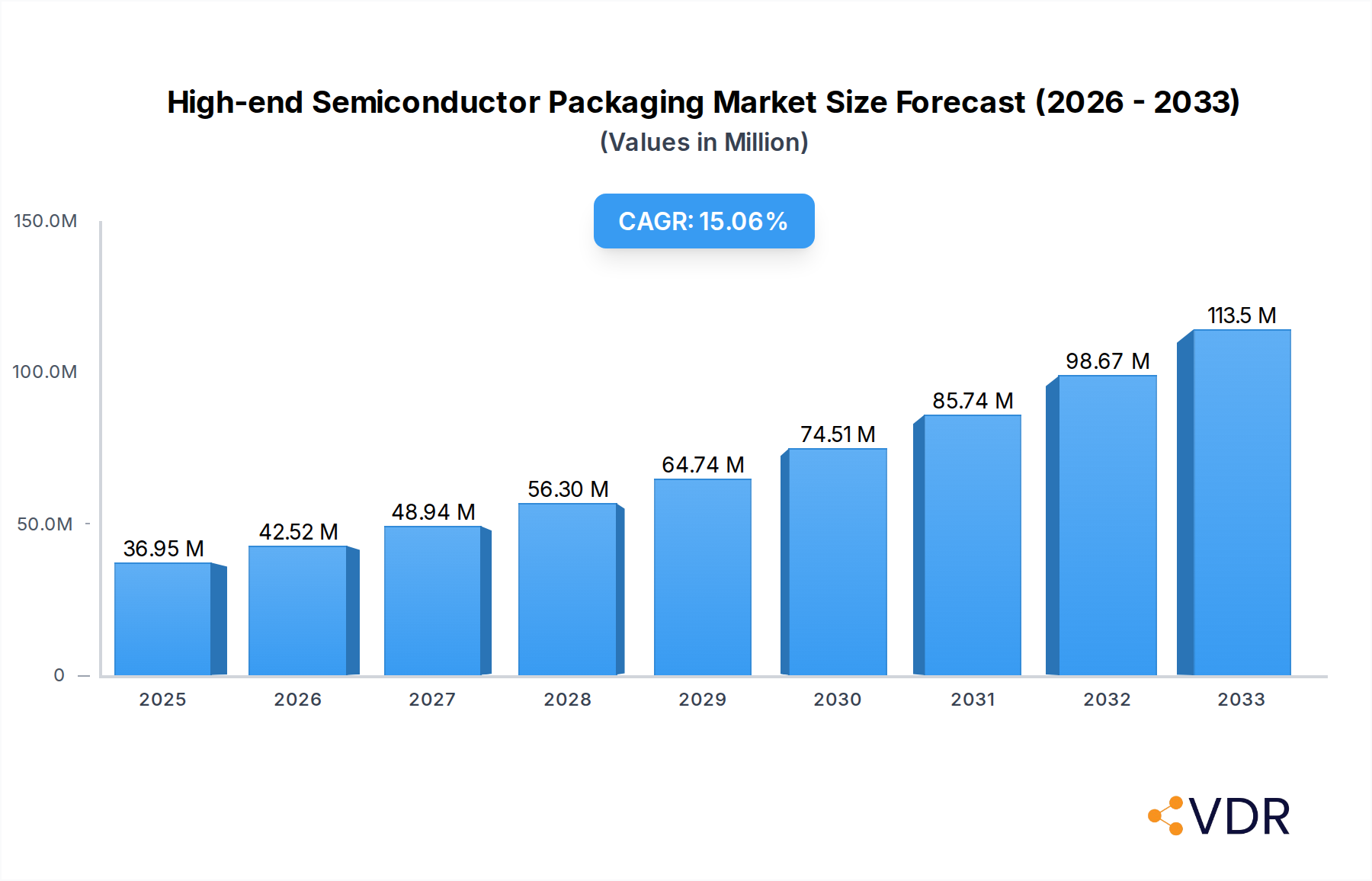
High-end Semiconductor Packaging Market Market Size (In Million)
The competitive landscape features prominent players including Taiwan Semiconductor Manufacturing Company, Samsung Electronics Co Ltd, and Advanced Semiconductor Engineering Inc., alongside other key contributors like Siliconware Precision Industries Co Ltd, Amkor Technology Inc., and Intel Corporation. These companies are actively investing in research and development to innovate and offer cutting-edge packaging solutions. While the market presents immense opportunities, potential restraints such as the high cost of advanced packaging technologies and the intricate supply chain management can pose challenges. However, the continuous technological advancements and the growing need for higher bandwidth and lower latency in data processing are expected to outweigh these challenges, ensuring sustained market growth throughout the forecast period. The increasing integration of artificial intelligence (AI) and machine learning (ML) across devices further amplifies the demand for high-performance semiconductor packaging.

High-end Semiconductor Packaging Market Company Market Share
High-end Semiconductor Packaging Market Report: Advanced Solutions for Next-Gen Electronics
This comprehensive report delves into the dynamic High-end Semiconductor Packaging Market, a critical enabler of advanced electronics. Explore the intricate landscape of advanced packaging solutions, including 3D SoC packaging, 3D stacked memory, 2.5D interposers, UHD FO packaging, and embedded Si bridge technology. We analyze the profound impact of these technologies across key end-user segments such as Consumer Electronics, Aerospace and Defense, Medical Devices, Telecom and Communication, and Automotive. This report provides an in-depth outlook for the High-end Semiconductor Packaging Market from 2019 to 2033, with a base year of 2025 and a forecast period of 2025–2033.
High-end Semiconductor Packaging Market Market Dynamics & Structure
The High-end Semiconductor Packaging Market is characterized by intense technological innovation, driving rapid evolution and a highly competitive environment. Market concentration is moderate, with a few dominant players like Taiwan Semiconductor Manufacturing Company, Samsung Electronics Co Ltd, and Advanced Semiconductor Engineering Inc. leading the charge in advanced packaging technologies. The primary drivers of innovation stem from the relentless demand for increased processing power, reduced form factors, and enhanced energy efficiency across various end-user industries. These demands are fueled by the proliferation of AI, 5G, IoT devices, and high-performance computing. Regulatory frameworks, while evolving to encourage domestic chip manufacturing and R&D, can sometimes introduce complexities related to supply chain diversification and international trade. Competitive product substitutes are limited in the high-end segment due to the specialized nature of advanced packaging, but incremental improvements in existing technologies and the emergence of novel materials act as indirect competitive pressures.
- Market Concentration: Dominated by a few key players, but with increasing participation from specialized foundries and OSATs.
- Technological Innovation Drivers: Miniaturization, performance enhancement, power efficiency, and new application demands (AI, 5G, HPC).
- Regulatory Frameworks: Government initiatives for semiconductor self-sufficiency and R&D incentives are shaping the landscape.
- Competitive Product Substitutes: Primarily focused on evolutionary improvements in existing packaging technologies rather than disruptive alternatives.
- End-User Demographics: Diversified, with a strong emphasis on high-growth sectors like automotive, telecom, and consumer electronics.
- M&A Trends: Strategic acquisitions and partnerships are common to gain access to new technologies, talent, and market share. For instance, the market has seen significant investment in expanding manufacturing capabilities.
High-end Semiconductor Packaging Market Growth Trends & Insights
The High-end Semiconductor Packaging Market is poised for robust growth, driven by an insatiable demand for miniaturized, powerful, and energy-efficient electronic components. The market size evolution is directly correlated with the advancements in semiconductor technology, particularly in areas like Artificial Intelligence, 5G deployment, and the burgeoning Internet of Things (IoT). Adoption rates for advanced packaging techniques such as 3D SoC, 3D stacked memory, and 2.5D interposers are accelerating as manufacturers strive to overcome the physical limitations of traditional planar designs. Technological disruptions, including the development of novel materials and manufacturing processes, are continuously pushing the boundaries of what's possible, enabling higher transistor densities and improved thermal management. Consumer behavior shifts towards more sophisticated and portable devices further catalyze this growth, demanding smaller yet more powerful chips.
The compound annual growth rate (CAGR) for the High-end Semiconductor Packaging Market is projected to be substantial over the forecast period. Market penetration of advanced packaging solutions is expected to deepen across all key end-user segments. For example, the automotive sector's increasing reliance on complex ADAS systems and in-car infotainment is a significant growth accelerator. Similarly, the continuous innovation in smartphones and wearable devices within the consumer electronics segment fuels the demand for smaller and more integrated packaging solutions. The increasing complexity of AI workloads, requiring massive parallel processing, directly translates to a higher demand for advanced packaging that can integrate multiple dies efficiently. Furthermore, the push towards heterogeneous integration, where different types of chips are combined into a single package, is a key trend shaping the market. This approach allows for optimized performance and cost-effectiveness, driving the adoption of technologies like 2.5D interposers and embedded Si bridges.
The market is also witnessing a significant trend towards specialized packaging solutions tailored for specific applications. For instance, high-performance computing (HPC) requires packaging that can handle immense heat dissipation and provide ultra-low latency interconnections. The telecom sector's need for faster data transmission speeds and lower power consumption in base stations and user equipment also drives innovation in packaging. The increasing sophistication of medical devices, from implantable sensors to advanced diagnostic equipment, necessitates highly reliable and miniaturized packaging solutions. The High-end Semiconductor Packaging Market is therefore not just about scaling but also about specialized integration and performance optimization. The transition from traditional packaging methods to these advanced techniques is a fundamental shift that will continue to propel market expansion. The investment in R&D by leading companies and government initiatives supporting domestic chip production further solidify the positive growth trajectory.
Dominant Regions, Countries, or Segments in High-end Semiconductor Packaging Market
The High-end Semiconductor Packaging Market is experiencing significant growth and innovation, with several regions, countries, and technology segments playing pivotal roles. Globally, Asia-Pacific, particularly Taiwan and South Korea, continues to dominate the semiconductor manufacturing and packaging landscape, leveraging advanced infrastructure, skilled labor, and substantial government support. These regions are home to leading foundries and Outsourced Semiconductor Assembly and Test (OSAT) companies that are at the forefront of developing and implementing cutting-edge packaging technologies. The concentration of R&D efforts and manufacturing capabilities in this region makes it a critical hub for the entire semiconductor ecosystem.
Within the technology segments, 3D SoC (System on Chip) packaging and 3D stacked memory are emerging as significant growth drivers. The ability to stack multiple dies vertically allows for unprecedented integration and performance improvements, crucial for applications in high-performance computing, AI accelerators, and advanced mobile devices. 2.5D interposers, which enable the co-packaged integration of multiple chiplets, are also gaining substantial traction, particularly in the data center and AI market. These technologies offer a pathway to overcome the limitations of monolithic chip scaling. The increasing demand for higher resolutions and frame rates in displays is also boosting the adoption of UHD FO (Ultra High Definition Fan-Out) packaging.
In terms of end-user segments, Consumer Electronics remains a major driver, with the relentless demand for thinner, lighter, and more powerful devices like smartphones, laptops, and wearables pushing the boundaries of packaging innovation. The Telecom and Communication sector is another key growth engine, fueled by the rollout of 5G networks, which requires advanced packaging for base stations, modems, and mobile devices to handle higher data rates and lower latency. The Automotive industry is witnessing a rapid transformation with the advent of autonomous driving and advanced driver-assistance systems (ADAS), necessitating sophisticated and highly reliable semiconductor packaging for sensors, processors, and infotainment systems. The increasing integration of electronics in vehicles directly translates to a growing demand for advanced packaging solutions.
- Dominant Region: Asia-Pacific (Taiwan, South Korea)
- Key Drivers: Established semiconductor ecosystem, strong government support, presence of leading foundries and OSATs, significant R&D investment.
- Dominant Technology Segments:
- 3D SoC Packaging: Enabling unprecedented integration and performance for AI and HPC.
- 3D Stacked Memory: Crucial for high-bandwidth memory applications in advanced computing.
- 2.5D Interposers: Facilitating chiplet integration for modular and scalable designs.
- UHD FO Packaging: Driven by the demand for higher resolution displays and advanced imaging.
- Dominant End-User Segments:
- Consumer Electronics: Continuous demand for miniaturization and performance in mobile devices and wearables.
- Telecom and Communication: Essential for 5G infrastructure and advanced mobile connectivity.
- Automotive: Rapid adoption of complex electronic systems for autonomous driving and in-car connectivity.
High-end Semiconductor Packaging Market Product Landscape
The High-end Semiconductor Packaging Market is characterized by a landscape of highly sophisticated products designed to meet the exacting demands of advanced electronic systems. Innovations focus on achieving greater integration density, enhanced thermal performance, and superior electrical characteristics. Key product categories include advanced 3D packaging solutions like 3D SoC, which integrate logic and memory dies vertically to significantly reduce form factor and improve interconnect speeds. 3D stacked memory, such as High Bandwidth Memory (HBM), offers unprecedented memory bandwidth essential for AI and HPC applications. Furthermore, 2.5D interposers provide a platform for heterogeneous integration, allowing different types of chips (e.g., CPU, GPU, AI accelerators) to be co-packaged with high-speed interconnects. UHD FO packaging is crucial for high-resolution displays, offering superior electrical performance and miniaturization. Embedded Si Bridge technology is another critical advancement, enabling tighter integration and improved performance by embedding interconnections within the silicon substrate itself. These products represent the cutting edge of semiconductor packaging, enabling next-generation performance and functionality.
Key Drivers, Barriers & Challenges in High-end Semiconductor Packaging Market
Key Drivers:
The High-end Semiconductor Packaging Market is propelled by several powerful forces. The relentless demand for higher performance, increased functionality, and reduced power consumption in electronic devices is a primary driver. Advancements in artificial intelligence (AI), machine learning (ML), and high-performance computing (HPC) necessitate sophisticated packaging solutions capable of handling massive data processing and complex interconnections. The widespread adoption of 5G technology is creating a demand for advanced packaging in mobile devices and network infrastructure. Furthermore, the automotive industry's rapid electrification and the development of autonomous driving systems require highly reliable and compact packaging for various sensors and processors. Government initiatives and investments in semiconductor manufacturing and R&D, aimed at securing domestic supply chains, also act as significant growth accelerators.
Barriers & Challenges:
Despite the robust growth, the High-end Semiconductor Packaging Market faces significant barriers and challenges. The extremely high cost of developing and implementing advanced packaging technologies, including advanced materials, specialized equipment, and extensive R&D, presents a substantial financial hurdle. Supply chain complexities and the reliance on specialized materials and manufacturing processes can lead to bottlenecks and potential disruptions. The increasing thermal management challenges associated with densely integrated chips require innovative solutions, adding to development costs and complexity. Stringent quality control and reliability requirements, especially for critical applications like automotive and aerospace, demand rigorous testing and validation processes. Finally, the shortage of skilled engineers and technicians with expertise in advanced packaging technologies can limit manufacturing scalability and innovation speed.
Emerging Opportunities in High-end Semiconductor Packaging Market
Emerging opportunities in the High-end Semiconductor Packaging Market lie in specialized applications and the integration of novel materials. The burgeoning fields of edge AI, where processing power needs to be brought closer to the data source, present a significant avenue for compact and efficient packaging solutions. The growth of the Internet of Medical Things (IoMT) and wearable health monitoring devices requires miniaturized, high-reliability packaging with advanced sensing capabilities. Furthermore, the development of new materials, such as advanced substrates and dielectric materials, offers opportunities for improved performance, thermal management, and reduced costs. The increasing adoption of chiplet-based designs, enabled by advanced packaging, allows for greater design flexibility and faster time-to-market for complex systems. The demand for sustainable and energy-efficient packaging solutions is also an emerging trend that will drive innovation.
Growth Accelerators in the High-end Semiconductor Packaging Market Industry
Several key catalysts are accelerating the growth of the High-end Semiconductor Packaging Market. The continuous advancement in semiconductor lithography and wafer fabrication technologies creates a demand for complementary packaging solutions that can leverage these improvements. Strategic partnerships and collaborations between foundries, OSATs, and equipment manufacturers are crucial for co-developing and optimizing advanced packaging processes. The increasing focus on vertical integration by major fabless companies and IDMs, to gain better control over their supply chain and accelerate innovation, also fuels the demand for advanced packaging. Government incentives and investments in establishing domestic manufacturing capabilities, as seen in initiatives across the US, Europe, and Asia, are significant growth accelerators, fostering local ecosystems and driving technological development.
Key Players Shaping the High-end Semiconductor Packaging Market Market
- Siliconware Precision Industries Co Ltd
- Taiwan Semiconductor Manufacturing Company
- Samsung Electronics Co Ltd
- Powertech Technology Inc
- Fujitsu Limited
- JCET Group Co Ltd
- TongFu Microelectronics Co Ltd
- Advanced Semiconductor Engineering Inc
- Amkor Technology Inc
- Intel Corporation
Notable Milestones in High-end Semiconductor Packaging Market Sector
- November 2023: Amkor Technology Inc. unveiled its blueprint for a packaging and testing facility in Peoria, Arizona, committing around USD 2 billion. This strategic investment aims to bolster high-performance computing, automotive, and communications sectors, underscoring Amkor's commitment to expanding its footprint in the dynamic semiconductor landscape.
- March 2023: Samsung Electronics announced plans to invest a significant USD 230 billion over the next two decades to establish the world's largest chip manufacturing hub. This initiative aligns with national strategies to elevate the chip industry, offering tax incentives and support to enhance the competitive edge of key high-tech sectors like chips, displays, and batteries.
In-Depth High-end Semiconductor Packaging Market Market Outlook
The future outlook for the High-end Semiconductor Packaging Market is exceptionally promising, driven by the pervasive integration of advanced semiconductor technologies across all facets of modern life. The continued evolution of AI, edge computing, and 5G is creating an insatiable demand for packaging that can deliver unparalleled performance, power efficiency, and miniaturization. Strategic investments in R&D and manufacturing capabilities by key industry players, coupled with supportive government policies, are creating a fertile ground for innovation and expansion. The trend towards heterogeneous integration, enabling the creation of highly specialized chiplet-based systems, will further fuel the adoption of advanced packaging solutions. Emerging opportunities in sectors like advanced medical devices and the burgeoning metaverse will also contribute significantly to market growth. The industry is on a trajectory of sustained expansion, driven by technological breakthroughs and evolving market needs.
High-end Semiconductor Packaging Market Segmentation
-
1. Technology
- 1.1. 3D SoC
- 1.2. 3D Stacked Memory
- 1.3. 2.5D interposers
- 1.4. UHD FO
- 1.5. Embedded Si Bridge
-
2. End User
- 2.1. Consumer Electronics
- 2.2. Aerospace and Defense
- 2.3. Medical Devices
- 2.4. Telecom and Communication
- 2.5. Automotive
- 2.6. Other End Users
High-end Semiconductor Packaging Market Segmentation By Geography
-
1. North America
- 1.1. United States
- 1.2. Canada
-
2. Europe
- 2.1. United Kingdom
- 2.2. Germany
- 2.3. France
- 2.4. Italy
-
3. Asia
- 3.1. China
- 3.2. India
- 3.3. Japan
- 3.4. Australia and New Zealand
- 3.5. South East Asia
- 4. Latin America
- 5. Middle East and Africa
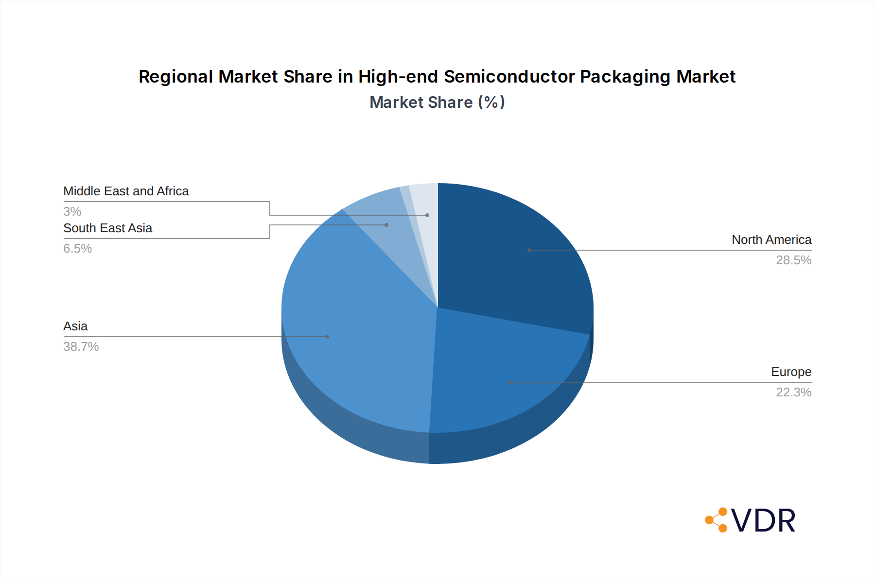
High-end Semiconductor Packaging Market Regional Market Share
Geographic Coverage of High-end Semiconductor Packaging Market
High-end Semiconductor Packaging Market REPORT HIGHLIGHTS
| Aspects | Details |
|---|---|
| Study Period | 2020-2034 |
| Base Year | 2025 |
| Estimated Year | 2026 |
| Forecast Period | 2026-2034 |
| Historical Period | 2020-2025 |
| Growth Rate | CAGR of 15.10% from 2020-2034 |
| Segmentation |
|
Table of Contents
- 1. Introduction
- 1.1. Research Scope
- 1.2. Market Segmentation
- 1.3. Research Objective
- 1.4. Definitions and Assumptions
- 2. Executive Summary
- 2.1. Market Snapshot
- 3. Market Dynamics
- 3.1. Market Drivers
- 3.2. Market Restrains
- 3.3. Market Trends
- 3.4. Market Opportunities
- 4. Market Factor Analysis
- 4.1. Porters Five Forces
- 4.1.1. Bargaining Power of Suppliers
- 4.1.2. Bargaining Power of Buyers
- 4.1.3. Threat of New Entrants
- 4.1.4. Threat of Substitutes
- 4.1.5. Competitive Rivalry
- 4.2. PESTEL analysis
- 4.3. BCG Analysis
- 4.3.1. Stars (High Growth, High Market Share)
- 4.3.2. Cash Cows (Low Growth, High Market Share)
- 4.3.3. Question Mark (High Growth, Low Market Share)
- 4.3.4. Dogs (Low Growth, Low Market Share)
- 4.4. Ansoff Matrix Analysis
- 4.5. Supply Chain Analysis
- 4.6. Regulatory Landscape
- 4.7. Current Market Potential and Opportunity Assessment (TAM–SAM–SOM Framework)
- 4.8. VDR Analyst Note
- 4.1. Porters Five Forces
- 5. Market Analysis, Insights and Forecast 2021-2033
- 5.1. Market Analysis, Insights and Forecast - by Technology
- 5.1.1. 3D SoC
- 5.1.2. 3D Stacked Memory
- 5.1.3. 2.5D interposers
- 5.1.4. UHD FO
- 5.1.5. Embedded Si Bridge
- 5.2. Market Analysis, Insights and Forecast - by End User
- 5.2.1. Consumer Electronics
- 5.2.2. Aerospace and Defense
- 5.2.3. Medical Devices
- 5.2.4. Telecom and Communication
- 5.2.5. Automotive
- 5.2.6. Other End Users
- 5.3. Market Analysis, Insights and Forecast - by Region
- 5.3.1. North America
- 5.3.2. Europe
- 5.3.3. Asia
- 5.3.4. Latin America
- 5.3.5. Middle East and Africa
- 5.1. Market Analysis, Insights and Forecast - by Technology
- 6. Global High-end Semiconductor Packaging Market Analysis, Insights and Forecast, 2021-2033
- 6.1. Market Analysis, Insights and Forecast - by Technology
- 6.1.1. 3D SoC
- 6.1.2. 3D Stacked Memory
- 6.1.3. 2.5D interposers
- 6.1.4. UHD FO
- 6.1.5. Embedded Si Bridge
- 6.2. Market Analysis, Insights and Forecast - by End User
- 6.2.1. Consumer Electronics
- 6.2.2. Aerospace and Defense
- 6.2.3. Medical Devices
- 6.2.4. Telecom and Communication
- 6.2.5. Automotive
- 6.2.6. Other End Users
- 6.1. Market Analysis, Insights and Forecast - by Technology
- 7. North America High-end Semiconductor Packaging Market Analysis, Insights and Forecast, 2021-2033
- 7.1. Market Analysis, Insights and Forecast - by Technology
- 7.1.1. 3D SoC
- 7.1.2. 3D Stacked Memory
- 7.1.3. 2.5D interposers
- 7.1.4. UHD FO
- 7.1.5. Embedded Si Bridge
- 7.2. Market Analysis, Insights and Forecast - by End User
- 7.2.1. Consumer Electronics
- 7.2.2. Aerospace and Defense
- 7.2.3. Medical Devices
- 7.2.4. Telecom and Communication
- 7.2.5. Automotive
- 7.2.6. Other End Users
- 7.1. Market Analysis, Insights and Forecast - by Technology
- 8. Europe High-end Semiconductor Packaging Market Analysis, Insights and Forecast, 2021-2033
- 8.1. Market Analysis, Insights and Forecast - by Technology
- 8.1.1. 3D SoC
- 8.1.2. 3D Stacked Memory
- 8.1.3. 2.5D interposers
- 8.1.4. UHD FO
- 8.1.5. Embedded Si Bridge
- 8.2. Market Analysis, Insights and Forecast - by End User
- 8.2.1. Consumer Electronics
- 8.2.2. Aerospace and Defense
- 8.2.3. Medical Devices
- 8.2.4. Telecom and Communication
- 8.2.5. Automotive
- 8.2.6. Other End Users
- 8.1. Market Analysis, Insights and Forecast - by Technology
- 9. Asia High-end Semiconductor Packaging Market Analysis, Insights and Forecast, 2021-2033
- 9.1. Market Analysis, Insights and Forecast - by Technology
- 9.1.1. 3D SoC
- 9.1.2. 3D Stacked Memory
- 9.1.3. 2.5D interposers
- 9.1.4. UHD FO
- 9.1.5. Embedded Si Bridge
- 9.2. Market Analysis, Insights and Forecast - by End User
- 9.2.1. Consumer Electronics
- 9.2.2. Aerospace and Defense
- 9.2.3. Medical Devices
- 9.2.4. Telecom and Communication
- 9.2.5. Automotive
- 9.2.6. Other End Users
- 9.1. Market Analysis, Insights and Forecast - by Technology
- 10. Latin America High-end Semiconductor Packaging Market Analysis, Insights and Forecast, 2021-2033
- 10.1. Market Analysis, Insights and Forecast - by Technology
- 10.1.1. 3D SoC
- 10.1.2. 3D Stacked Memory
- 10.1.3. 2.5D interposers
- 10.1.4. UHD FO
- 10.1.5. Embedded Si Bridge
- 10.2. Market Analysis, Insights and Forecast - by End User
- 10.2.1. Consumer Electronics
- 10.2.2. Aerospace and Defense
- 10.2.3. Medical Devices
- 10.2.4. Telecom and Communication
- 10.2.5. Automotive
- 10.2.6. Other End Users
- 10.1. Market Analysis, Insights and Forecast - by Technology
- 11. Middle East and Africa High-end Semiconductor Packaging Market Analysis, Insights and Forecast, 2021-2033
- 11.1. Market Analysis, Insights and Forecast - by Technology
- 11.1.1. 3D SoC
- 11.1.2. 3D Stacked Memory
- 11.1.3. 2.5D interposers
- 11.1.4. UHD FO
- 11.1.5. Embedded Si Bridge
- 11.2. Market Analysis, Insights and Forecast - by End User
- 11.2.1. Consumer Electronics
- 11.2.2. Aerospace and Defense
- 11.2.3. Medical Devices
- 11.2.4. Telecom and Communication
- 11.2.5. Automotive
- 11.2.6. Other End Users
- 11.1. Market Analysis, Insights and Forecast - by Technology
- 12. Competitive Analysis
- 12.1. Company Profiles
- 12.1.1 Siliconware Precision Industries Co Ltd
- 12.1.1.1. Company Overview
- 12.1.1.2. Products
- 12.1.1.3. Company Financials
- 12.1.1.4. SWOT Analysis
- 12.1.2 Taiwan Semiconductor Manufacturing Company
- 12.1.2.1. Company Overview
- 12.1.2.2. Products
- 12.1.2.3. Company Financials
- 12.1.2.4. SWOT Analysis
- 12.1.3 Samsung Electronics Co Ltd
- 12.1.3.1. Company Overview
- 12.1.3.2. Products
- 12.1.3.3. Company Financials
- 12.1.3.4. SWOT Analysis
- 12.1.4 Powertech Technology Inc *List Not Exhaustive
- 12.1.4.1. Company Overview
- 12.1.4.2. Products
- 12.1.4.3. Company Financials
- 12.1.4.4. SWOT Analysis
- 12.1.5 Fujitsu Limited
- 12.1.5.1. Company Overview
- 12.1.5.2. Products
- 12.1.5.3. Company Financials
- 12.1.5.4. SWOT Analysis
- 12.1.6 JCET Group Co Ltd
- 12.1.6.1. Company Overview
- 12.1.6.2. Products
- 12.1.6.3. Company Financials
- 12.1.6.4. SWOT Analysis
- 12.1.7 TongFu Microelectronics Co Ltd
- 12.1.7.1. Company Overview
- 12.1.7.2. Products
- 12.1.7.3. Company Financials
- 12.1.7.4. SWOT Analysis
- 12.1.8 Advanced Semiconductor Engineering Inc
- 12.1.8.1. Company Overview
- 12.1.8.2. Products
- 12.1.8.3. Company Financials
- 12.1.8.4. SWOT Analysis
- 12.1.9 Amkor Technology Inc
- 12.1.9.1. Company Overview
- 12.1.9.2. Products
- 12.1.9.3. Company Financials
- 12.1.9.4. SWOT Analysis
- 12.1.10 Intel Corporation
- 12.1.10.1. Company Overview
- 12.1.10.2. Products
- 12.1.10.3. Company Financials
- 12.1.10.4. SWOT Analysis
- 12.1.1 Siliconware Precision Industries Co Ltd
- 12.2. Market Entropy
- 12.2.1 Company's Key Areas Served
- 12.2.2 Recent Developments
- 12.3. Company Market Share Analysis 2025
- 12.3.1 Top 5 Companies Market Share Analysis
- 12.3.2 Top 3 Companies Market Share Analysis
- 12.4. List of Potential Customers
- 13. Research Methodology
List of Figures
- Figure 1: Global High-end Semiconductor Packaging Market Revenue Breakdown (Million, %) by Region 2025 & 2033
- Figure 2: North America High-end Semiconductor Packaging Market Revenue (Million), by Technology 2025 & 2033
- Figure 3: North America High-end Semiconductor Packaging Market Revenue Share (%), by Technology 2025 & 2033
- Figure 4: North America High-end Semiconductor Packaging Market Revenue (Million), by End User 2025 & 2033
- Figure 5: North America High-end Semiconductor Packaging Market Revenue Share (%), by End User 2025 & 2033
- Figure 6: North America High-end Semiconductor Packaging Market Revenue (Million), by Country 2025 & 2033
- Figure 7: North America High-end Semiconductor Packaging Market Revenue Share (%), by Country 2025 & 2033
- Figure 8: Europe High-end Semiconductor Packaging Market Revenue (Million), by Technology 2025 & 2033
- Figure 9: Europe High-end Semiconductor Packaging Market Revenue Share (%), by Technology 2025 & 2033
- Figure 10: Europe High-end Semiconductor Packaging Market Revenue (Million), by End User 2025 & 2033
- Figure 11: Europe High-end Semiconductor Packaging Market Revenue Share (%), by End User 2025 & 2033
- Figure 12: Europe High-end Semiconductor Packaging Market Revenue (Million), by Country 2025 & 2033
- Figure 13: Europe High-end Semiconductor Packaging Market Revenue Share (%), by Country 2025 & 2033
- Figure 14: Asia High-end Semiconductor Packaging Market Revenue (Million), by Technology 2025 & 2033
- Figure 15: Asia High-end Semiconductor Packaging Market Revenue Share (%), by Technology 2025 & 2033
- Figure 16: Asia High-end Semiconductor Packaging Market Revenue (Million), by End User 2025 & 2033
- Figure 17: Asia High-end Semiconductor Packaging Market Revenue Share (%), by End User 2025 & 2033
- Figure 18: Asia High-end Semiconductor Packaging Market Revenue (Million), by Country 2025 & 2033
- Figure 19: Asia High-end Semiconductor Packaging Market Revenue Share (%), by Country 2025 & 2033
- Figure 20: Latin America High-end Semiconductor Packaging Market Revenue (Million), by Technology 2025 & 2033
- Figure 21: Latin America High-end Semiconductor Packaging Market Revenue Share (%), by Technology 2025 & 2033
- Figure 22: Latin America High-end Semiconductor Packaging Market Revenue (Million), by End User 2025 & 2033
- Figure 23: Latin America High-end Semiconductor Packaging Market Revenue Share (%), by End User 2025 & 2033
- Figure 24: Latin America High-end Semiconductor Packaging Market Revenue (Million), by Country 2025 & 2033
- Figure 25: Latin America High-end Semiconductor Packaging Market Revenue Share (%), by Country 2025 & 2033
- Figure 26: Middle East and Africa High-end Semiconductor Packaging Market Revenue (Million), by Technology 2025 & 2033
- Figure 27: Middle East and Africa High-end Semiconductor Packaging Market Revenue Share (%), by Technology 2025 & 2033
- Figure 28: Middle East and Africa High-end Semiconductor Packaging Market Revenue (Million), by End User 2025 & 2033
- Figure 29: Middle East and Africa High-end Semiconductor Packaging Market Revenue Share (%), by End User 2025 & 2033
- Figure 30: Middle East and Africa High-end Semiconductor Packaging Market Revenue (Million), by Country 2025 & 2033
- Figure 31: Middle East and Africa High-end Semiconductor Packaging Market Revenue Share (%), by Country 2025 & 2033
List of Tables
- Table 1: Global High-end Semiconductor Packaging Market Revenue Million Forecast, by Technology 2020 & 2033
- Table 2: Global High-end Semiconductor Packaging Market Revenue Million Forecast, by End User 2020 & 2033
- Table 3: Global High-end Semiconductor Packaging Market Revenue Million Forecast, by Region 2020 & 2033
- Table 4: Global High-end Semiconductor Packaging Market Revenue Million Forecast, by Technology 2020 & 2033
- Table 5: Global High-end Semiconductor Packaging Market Revenue Million Forecast, by End User 2020 & 2033
- Table 6: Global High-end Semiconductor Packaging Market Revenue Million Forecast, by Country 2020 & 2033
- Table 7: United States High-end Semiconductor Packaging Market Revenue (Million) Forecast, by Application 2020 & 2033
- Table 8: Canada High-end Semiconductor Packaging Market Revenue (Million) Forecast, by Application 2020 & 2033
- Table 9: Global High-end Semiconductor Packaging Market Revenue Million Forecast, by Technology 2020 & 2033
- Table 10: Global High-end Semiconductor Packaging Market Revenue Million Forecast, by End User 2020 & 2033
- Table 11: Global High-end Semiconductor Packaging Market Revenue Million Forecast, by Country 2020 & 2033
- Table 12: United Kingdom High-end Semiconductor Packaging Market Revenue (Million) Forecast, by Application 2020 & 2033
- Table 13: Germany High-end Semiconductor Packaging Market Revenue (Million) Forecast, by Application 2020 & 2033
- Table 14: France High-end Semiconductor Packaging Market Revenue (Million) Forecast, by Application 2020 & 2033
- Table 15: Italy High-end Semiconductor Packaging Market Revenue (Million) Forecast, by Application 2020 & 2033
- Table 16: Global High-end Semiconductor Packaging Market Revenue Million Forecast, by Technology 2020 & 2033
- Table 17: Global High-end Semiconductor Packaging Market Revenue Million Forecast, by End User 2020 & 2033
- Table 18: Global High-end Semiconductor Packaging Market Revenue Million Forecast, by Country 2020 & 2033
- Table 19: China High-end Semiconductor Packaging Market Revenue (Million) Forecast, by Application 2020 & 2033
- Table 20: India High-end Semiconductor Packaging Market Revenue (Million) Forecast, by Application 2020 & 2033
- Table 21: Japan High-end Semiconductor Packaging Market Revenue (Million) Forecast, by Application 2020 & 2033
- Table 22: Australia and New Zealand High-end Semiconductor Packaging Market Revenue (Million) Forecast, by Application 2020 & 2033
- Table 23: South East Asia High-end Semiconductor Packaging Market Revenue (Million) Forecast, by Application 2020 & 2033
- Table 24: Global High-end Semiconductor Packaging Market Revenue Million Forecast, by Technology 2020 & 2033
- Table 25: Global High-end Semiconductor Packaging Market Revenue Million Forecast, by End User 2020 & 2033
- Table 26: Global High-end Semiconductor Packaging Market Revenue Million Forecast, by Country 2020 & 2033
- Table 27: Global High-end Semiconductor Packaging Market Revenue Million Forecast, by Technology 2020 & 2033
- Table 28: Global High-end Semiconductor Packaging Market Revenue Million Forecast, by End User 2020 & 2033
- Table 29: Global High-end Semiconductor Packaging Market Revenue Million Forecast, by Country 2020 & 2033
Frequently Asked Questions
1. What is the projected Compound Annual Growth Rate (CAGR) of the High-end Semiconductor Packaging Market?
The projected CAGR is approximately 15.10%.
2. Which companies are prominent players in the High-end Semiconductor Packaging Market?
Key companies in the market include Siliconware Precision Industries Co Ltd, Taiwan Semiconductor Manufacturing Company, Samsung Electronics Co Ltd, Powertech Technology Inc *List Not Exhaustive, Fujitsu Limited, JCET Group Co Ltd, TongFu Microelectronics Co Ltd, Advanced Semiconductor Engineering Inc, Amkor Technology Inc, Intel Corporation.
3. What are the main segments of the High-end Semiconductor Packaging Market?
The market segments include Technology, End User.
4. Can you provide details about the market size?
The market size is estimated to be USD 36.95 Million as of 2022.
5. What are some drivers contributing to market growth?
Growing Consumption of Semiconductor Devices Across Industries; Growing Adoption of 3D Printing in Semiconductor Packaging.
6. What are the notable trends driving market growth?
Consumer Electronics Sector is Expected to Boost the Market.
7. Are there any restraints impacting market growth?
High Initial Investment and Increasing Complexity of Semiconductor IC Designs.
8. Can you provide examples of recent developments in the market?
November 2023: Amkor Technology Inc., a provider of semiconductor packaging and testing services, unveiled its blueprint for a packaging and testing facility in Peoria, Arizona. The company is set to channel around USD 2 billion into the project. Amkor aims to bolster key sectors like high-performance computing, automotive, and communications. This move underscores Amkor's commitment to deepening its roots in the dynamic semiconductor landscape.
9. What pricing options are available for accessing the report?
Pricing options include single-user, multi-user, and enterprise licenses priced at USD 4750, USD 5250, and USD 8750 respectively.
10. Is the market size provided in terms of value or volume?
The market size is provided in terms of value, measured in Million.
11. Are there any specific market keywords associated with the report?
Yes, the market keyword associated with the report is "High-end Semiconductor Packaging Market," which aids in identifying and referencing the specific market segment covered.
12. How do I determine which pricing option suits my needs best?
The pricing options vary based on user requirements and access needs. Individual users may opt for single-user licenses, while businesses requiring broader access may choose multi-user or enterprise licenses for cost-effective access to the report.
13. Are there any additional resources or data provided in the High-end Semiconductor Packaging Market report?
While the report offers comprehensive insights, it's advisable to review the specific contents or supplementary materials provided to ascertain if additional resources or data are available.
14. How can I stay updated on further developments or reports in the High-end Semiconductor Packaging Market?
To stay informed about further developments, trends, and reports in the High-end Semiconductor Packaging Market, consider subscribing to industry newsletters, following relevant companies and organizations, or regularly checking reputable industry news sources and publications.
Methodology
Step 1 - Identification of Relevant Samples Size from Population Database

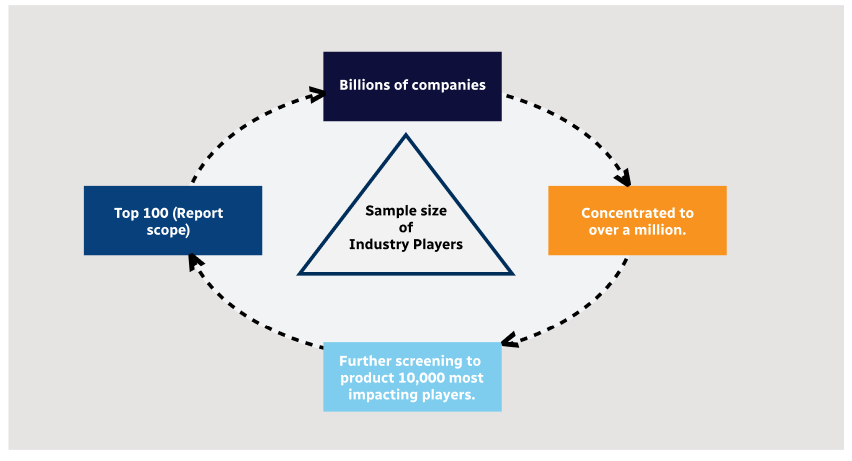
Step 2 - Approaches for Defining Global Market Size (Value, Volume* & Price*)
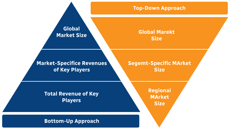
Note*: In applicable scenarios
Step 3 - Data Sources
Primary Research
- Web Analytics
- Survey Reports
- Research Institute
- Latest Research Reports
- Opinion Leaders
Secondary Research
- Annual Reports
- White Paper
- Latest Press Release
- Industry Association
- Paid Database
- Investor Presentations

Step 4 - Data Triangulation
Involves using different sources of information in order to increase the validity of a study
These sources are likely to be stakeholders in a program - participants, other researchers, program staff, other community members, and so on.
Then we put all data in single framework & apply various statistical tools to find out the dynamic on the market.
During the analysis stage, feedback from the stakeholder groups would be compared to determine areas of agreement as well as areas of divergence