

Key Insights
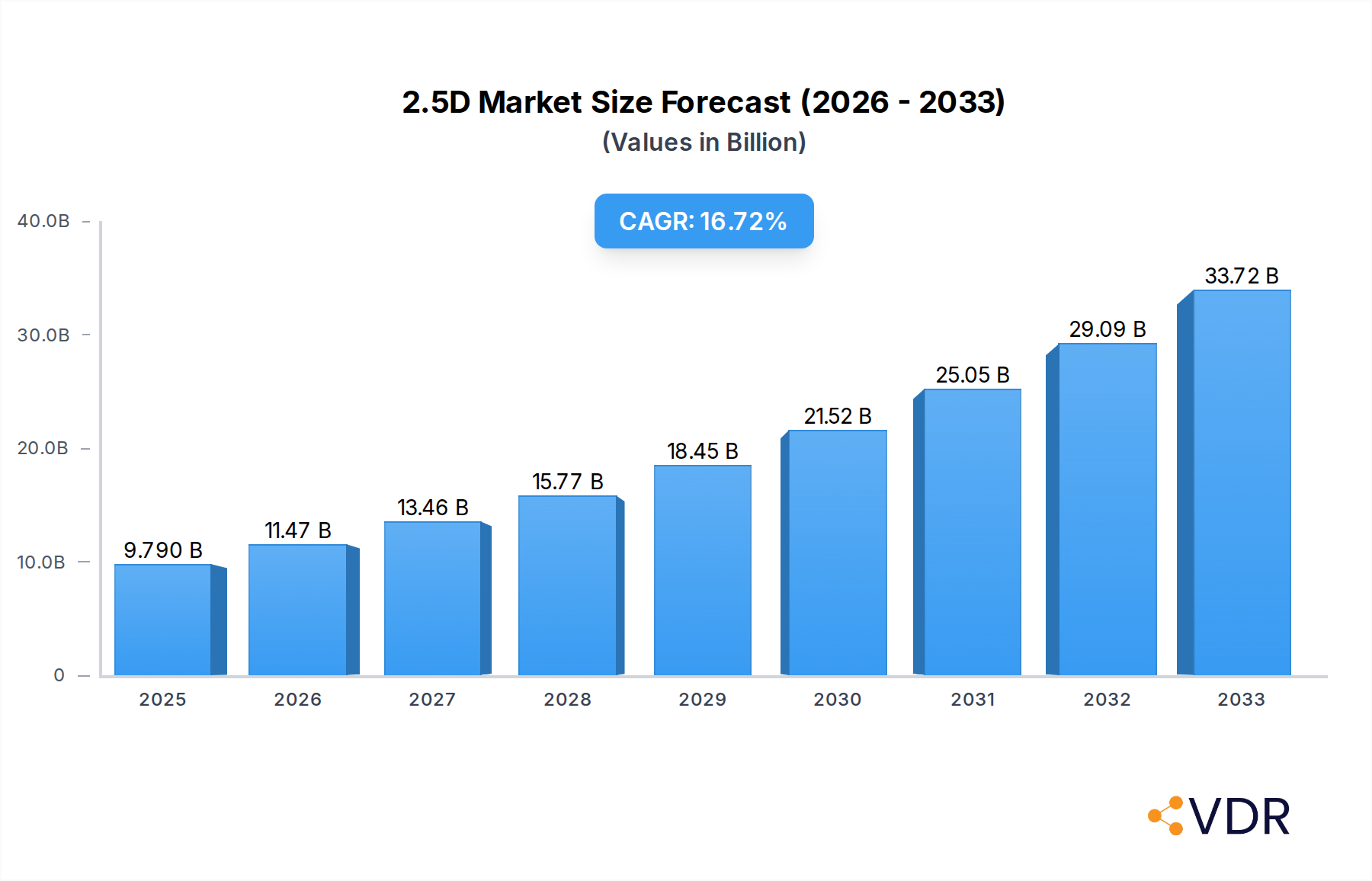
The 2.5D & 3D Semiconductor Packaging Industry is poised for significant expansion, driven by the relentless demand for higher performance, miniaturization, and increased functionality in electronic devices. The market is projected to reach an impressive $9.79 Billion by 2025, demonstrating a robust compound annual growth rate (CAGR) of 17.20% through 2033. This surge is fueled by critical drivers such as the escalating adoption of advanced technologies like artificial intelligence (AI), machine learning (ML), and the Internet of Things (IoT), all of which necessitate sophisticated packaging solutions to integrate multiple chips and enhance data processing capabilities. The automotive sector, with its increasing reliance on advanced driver-assistance systems (ADAS) and autonomous driving technology, is a major contributor to this growth. Similarly, the medical device industry's push for smaller, more powerful, and integrated diagnostic and therapeutic systems is also a key enabler. The consumer electronics market continues to innovate with demands for faster processors, better graphics, and longer battery life, directly benefiting from the density and performance gains offered by 2.5D and 3D packaging.

2.5D & 3D Semiconductor Packaging Industry Market Size (In Billion)
Emerging trends like heterogeneous integration, where different types of chips are combined within a single package, are at the forefront of this market's evolution. This approach allows for optimized performance and reduced form factors, catering to the stringent requirements of next-generation devices. The development of advanced wafer-level packaging techniques and the increasing complexity of chip designs are further propelling the industry forward. While the market is experiencing substantial growth, it faces certain restraints. These include the high cost associated with developing and implementing these advanced packaging technologies, as well as the need for specialized manufacturing equipment and skilled labor. Supply chain complexities and the potential for yield issues in intricate multi-chip assemblies also present challenges. However, the continuous innovation by leading companies like Samsung Electronics, ASE Group, and TSMC, coupled with the ongoing research and development in materials and manufacturing processes, are expected to mitigate these restraints and ensure sustained market expansion. The industry's focus on enhancing thermal management and improving interconnectivity within these advanced packages will be crucial for unlocking their full potential.
2.5D & 3D Semiconductor Packaging Industry Company Market Share
Unlocking the Future of Computing: 2.5D & 3D Semiconductor Packaging Industry Report | 2019-2033
This comprehensive market research report provides an in-depth analysis of the 2.5D & 3D semiconductor packaging industry, offering critical insights into market dynamics, growth trends, regional dominance, product landscape, key drivers, barriers, emerging opportunities, growth accelerators, and leading players. Spanning the historical period of 2019-2024 and projecting future growth through 2033, with a base year of 2025, this report is an indispensable resource for stakeholders seeking to navigate and capitalize on this rapidly evolving sector. We delve into both parent and child market segments, providing granular detail on advanced semiconductor packaging solutions.
Keywords: 2.5D Packaging, 3D Packaging, Advanced Semiconductor Packaging, Semiconductor Packaging Market, Chiplets, Heterogeneous Integration, High-Performance Computing (HPC), Artificial Intelligence (AI), 5G, Automotive Electronics, Consumer Electronics, Medical Devices, TSV (Through-Silicon Via), EMIB, Wafer Level Packaging, Fan-Out Packaging, System-in-Package (SiP), Semiconductor Manufacturing, Microelectronics, Silicon Photonics, Photonics Packaging, Quantum Computing, Edge AI, Generative AI, Next-Gen Processors, Memory Packaging, Logic Packaging, GPU Packaging, CPU Packaging, Data Centers, Wearable Technology, IoT Devices.
2.5D & 3D Semiconductor Packaging Industry Market Dynamics & Structure
The 2.5D & 3D semiconductor packaging industry is characterized by a moderate to high market concentration, driven by significant technological innovation and substantial capital investment. Key players like Samsung Electronics Co Ltd, ASE Group, TSMC Limited, and Intel Corporation dominate the landscape, investing heavily in research and development to push the boundaries of miniaturization and performance. Technological innovation is primarily fueled by the increasing demand for higher processing power, reduced power consumption, and smaller form factors across diverse end-user industries. The industry is also shaped by evolving regulatory frameworks, particularly concerning supply chain resilience and environmental sustainability. Competitive product substitutes, such as advanced 2D packaging solutions and novel materials, continuously emerge, pushing for greater innovation. End-user demographics are increasingly driven by the proliferation of AI, HPC, 5G, and IoT devices, demanding more sophisticated and integrated packaging solutions. Mergers and acquisitions (M&A) trends are notable, as companies seek to consolidate capabilities, gain market share, and access new technologies. For instance, strategic partnerships and acquisitions are common to secure intellectual property and expand manufacturing capacity, with an estimated XX M&A deal volumes in the historical period. The barriers to innovation are significant, including the complexity of manufacturing processes, high development costs, and the need for specialized equipment.
- Market Concentration: Dominated by a few key players with substantial R&D budgets and manufacturing capabilities.
- Technological Innovation Drivers: Demand for higher performance, lower power consumption, miniaturization, and heterogeneous integration.
- Regulatory Frameworks: Increasing focus on supply chain security, geopolitical considerations, and environmental impact.
- Competitive Product Substitutes: Advanced 2D packaging, novel material science, and emerging interconnect technologies.
- End-User Demographics: Proliferation of AI, HPC, 5G, Automotive, Medical Devices, and Consumer Electronics driving demand.
- M&A Trends: Strategic acquisitions and partnerships to gain market share, technology access, and expand manufacturing footprint.
- Innovation Barriers: High R&D costs, complex manufacturing processes, skilled labor shortage, and stringent quality control requirements.
2.5D & 3D Semiconductor Packaging Industry Growth Trends & Insights
The 2.5D & 3D semiconductor packaging industry is poised for robust growth, driven by the insatiable demand for enhanced performance and efficiency in electronic devices. The market size evolution shows a consistent upward trajectory, with the base year 2025 estimated at USD $XX billion. The adoption rates of 2.5D and 3D packaging technologies are accelerating, propelled by their ability to integrate multiple dies (chiplets) and functionalities into a single package, leading to significant improvements in speed, power efficiency, and reduced physical footprint. Technological disruptions, such as the rise of chiplet architectures and advanced interconnect technologies like EMIB and TSV, are fundamentally reshaping the industry. Consumer behavior shifts towards more powerful, compact, and energy-efficient devices, from smartphones and wearables to high-performance computing systems and autonomous vehicles, are directly fueling this growth. The projected Compound Annual Growth Rate (CAGR) for the forecast period 2025–2033 is estimated at XX%, reaching an estimated market size of USD $XX billion by 2033. Market penetration is deepening across key sectors, with significant advancements in integrating logic, memory, and specialized accelerators. The ability to achieve higher bandwidth and lower latency through these advanced packaging techniques is becoming critical for applications like artificial intelligence, machine learning, and real-time data processing. Furthermore, the increasing complexity of semiconductor designs and the physical limitations of traditional 2D scaling are compelling manufacturers to adopt these advanced 3D and 2.5D solutions as the primary path forward for performance enhancement. The integration of AI capabilities directly into edge devices and the burgeoning data center market for AI model training and inference are significant growth engines.
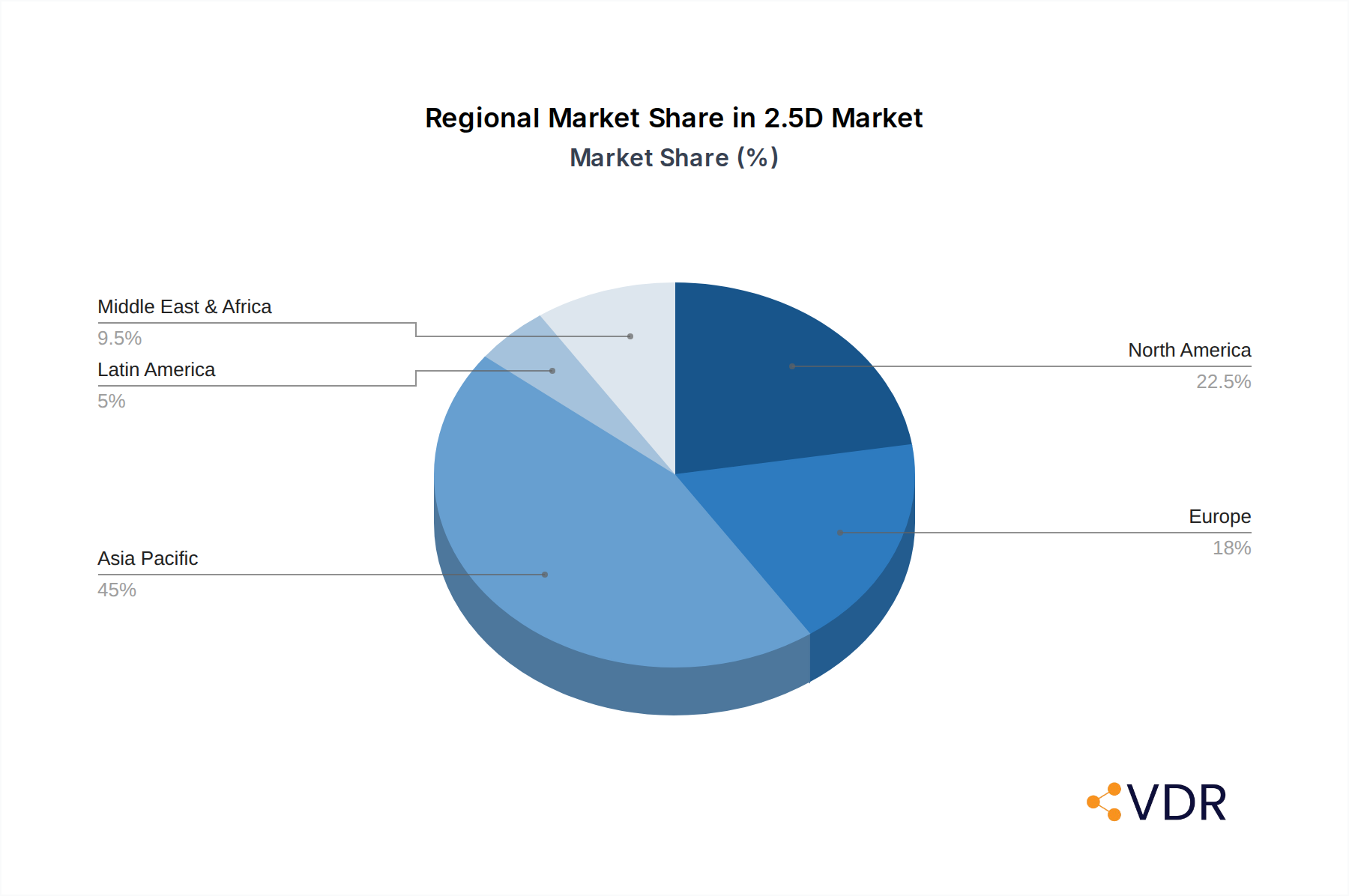
Dominant Regions, Countries, or Segments in 2.5D & 3D Semiconductor Packaging Industry
The 2.5D & 3D semiconductor packaging industry is experiencing dominant growth driven by key regions and segments that are at the forefront of technological innovation and demand. Asia Pacific, particularly Taiwan, South Korea, and China, stands out as the leading region. This dominance is attributed to the presence of major semiconductor foundries and packaging houses, significant government support for the semiconductor industry, a well-established supply chain, and a burgeoning demand from the electronics manufacturing hubs located within these countries.
Within the Packaging Technology segment, 2.5D packaging currently holds a significant market share, driven by its ability to integrate advanced logic and memory components with high-speed interconnects without the full complexity of through-silicon vias (TSVs). However, 3D packaging, including wafer-level 3D and stacked die solutions, is exhibiting a higher growth rate as technology matures and the demand for denser integration intensifies, particularly for memory-intensive applications like AI accelerators and high-bandwidth memory (HBM). The 3D Wafer technology is also gaining traction for its potential to create extremely compact and powerful integrated systems.
In terms of End-user Industries, Consumer Electronics remains a primary driver due to the relentless demand for more powerful smartphones, laptops, gaming consoles, and other personal devices. However, Communications and Telecom, fueled by the rollout of 5G infrastructure and the increasing complexity of network equipment, is witnessing rapid growth in the adoption of advanced packaging. The Automotive sector is another critical growth area, with the increasing sophistication of Advanced Driver-Assistance Systems (ADAS), infotainment systems, and the eventual widespread adoption of autonomous driving technologies necessitating highly reliable and performant semiconductor solutions that advanced packaging provides. The Medical Devices segment, with its growing reliance on miniaturized, high-performance electronics for diagnostic tools, implantable devices, and imaging equipment, also represents a significant and growing market for 2.5D and 3D packaging.
- Dominant Region: Asia Pacific (Taiwan, South Korea, China)
- Key Drivers: Presence of major foundries and OSATs (Outsourced Semiconductor Assembly and Test), strong government support, robust manufacturing ecosystem, high consumer electronics demand.
- Market Share: Holds the largest share of global semiconductor packaging production and R&D.
- Leading Packaging Technology:
- 2.5D Packaging: Currently dominant due to its balance of performance and cost-effectiveness for high-end applications like HPC and AI.
- 3D Packaging: Rapidly growing segment, especially for memory stacking (HBM) and stacked die solutions, enabling ultimate miniaturization and performance gains.
- Key End-User Industries:
- Consumer Electronics: Continuous demand for performance upgrades in personal devices.
- Communications and Telecom: Essential for 5G infrastructure, network processing, and high-speed data transmission.
- Automotive: Critical for ADAS, autonomous driving, and in-car electronics requiring high reliability and performance.
- Medical Devices: Enabling miniaturization and enhanced functionality in advanced healthcare equipment.
2.5D & 3D Semiconductor Packaging Industry Product Landscape
The product landscape of the 2.5D & 3D semiconductor packaging industry is defined by increasingly sophisticated integration techniques that enable enhanced performance, power efficiency, and reduced form factors. Key product innovations include advanced wafer-level packaging (WLP) technologies, such as fan-out wafer-level packaging (FOWLP), enabling the integration of multiple dies with integrated redistribution layers (RDLs). 2.5D packaging solutions leverage interposers, like silicon or organic substrates, to connect dies with high-density interconnects, facilitating heterogeneous integration of CPUs, GPUs, and memory. 3D packaging solutions, such as die stacking and through-silicon via (TSV) technology, allow for vertical integration of memory and logic, leading to significant improvements in bandwidth and latency. These packaging solutions are crucial for high-performance computing (HPC), artificial intelligence (AI) accelerators, and advanced networking equipment, offering unique selling propositions in terms of performance gains, power savings, and miniaturization.
Key Drivers, Barriers & Challenges in 2.5D & 3D Semiconductor Packaging Industry
The 2.5D & 3D semiconductor packaging industry is propelled by several key drivers, primarily the escalating demand for higher computing performance and miniaturization across all electronic sectors. The proliferation of artificial intelligence (AI), high-performance computing (HPC), 5G networks, and autonomous systems necessitates more advanced packaging solutions that can integrate multiple complex dies efficiently. Technological advancements in chiplet architectures and heterogeneous integration are also crucial drivers, enabling specialized functions to be combined seamlessly.
However, the industry faces significant barriers and challenges. The complexity and cost of manufacturing advanced 3D and 2.5D packaging solutions are substantial, requiring specialized equipment, intricate processes, and stringent quality control. Supply chain disruptions and the geopolitical landscape also pose considerable risks, impacting material availability and manufacturing continuity. Furthermore, the high power density within these integrated packages can lead to thermal management challenges, requiring innovative cooling solutions. The need for highly skilled labor in design, manufacturing, and testing further exacerbates these challenges.
- Key Drivers:
- Increasing demand for AI, HPC, 5G, and autonomous driving technologies.
- Advancements in chiplet architectures and heterogeneous integration.
- Need for improved performance, power efficiency, and reduced form factors.
- Limitations of traditional 2D scaling.
- Barriers & Challenges:
- High manufacturing complexity and cost.
- Supply chain vulnerabilities and geopolitical risks.
- Thermal management issues due to increased power density.
- Shortage of skilled workforce.
- Stringent reliability and quality assurance requirements.
Emerging Opportunities in 2.5D & 3D Semiconductor Packaging Industry
Emerging opportunities within the 2.5D & 3D semiconductor packaging industry are vast and transformative. The burgeoning field of AI is a significant opportunity, with the development of specialized AI accelerators and neural processing units (NPUs) that benefit immensely from the performance gains offered by 3D integration. The growth of edge computing and the Internet of Things (IoT) presents a demand for ultra-low-power, compact, and highly integrated packaging solutions for devices at the network's edge. Photonics packaging, integrating optical components with electronic chips, is another promising area, enabling faster data transfer and new applications in telecommunications and sensing. The advancements in quantum computing also hint at future demands for highly specialized and densely integrated packaging for quantum processors. Furthermore, the increasing trend towards co-design and co-optimization of chips and packages opens new avenues for innovation and performance enhancement.
Growth Accelerators in the 2.5D & 3D Semiconductor Packaging Industry Industry
Several catalysts are accelerating the long-term growth of the 2.5D & 3D semiconductor packaging industry. Continuous technological breakthroughs in materials science, such as advanced dielectrics and thermal interface materials, are enabling better performance and reliability. Strategic partnerships and collaborations between foundries, fabless design companies, and packaging manufacturers are fostering innovation and speeding up the adoption of new technologies. The expansion of semiconductor manufacturing capacity, particularly in emerging markets, will also play a crucial role. Moreover, the increasing standardization of chiplet interfaces and architectures is simplifying the integration process, making advanced packaging more accessible and appealing to a wider range of applications. The growing emphasis on sustainability and energy efficiency in electronics manufacturing is also pushing for more integrated and power-efficient packaging solutions.
Key Players Shaping the 2.5D & 3D Semiconductor Packaging Industry Market
- Samsung Electronics Co Ltd
- ASE Group
- TSMC Limited
- Jiangsu Changjiang Electronics Technology Co Ltd
- Tezzaron Semiconductor Corporation
- Powertech Technology Inc
- Siliconware Precision Industries Co Ltd (SPIL)
- Amkor Technology Inc
- Intel Corporation
- GlobalFoundries Inc
Notable Milestones in 2.5D & 3D Semiconductor Packaging Industry Sector
- February 2024: Ansys and Intel Foundry partnered to offer Multiphysics signoff solutions for Intel's advanced 2.5D chip assembly technology. This technology utilizes EMIB technology to connect the die flexibly without using through-silicon via (TSVs). Ansys' precise simulation engines provide improved speeds, reduced power consumption, and increased reliability in sophisticated silicon systems for artificial intelligence (AI), high-performance computing, autonomous driving, and graphic processing.
- November 2023: Samsung Electronics was preparing to launch a new advanced 3D chip packaging technology called SAINT (Samsung Advanced Interconnection Technology) to compete with Taiwan Semiconductor Manufacturing Company's (TSMC) dominance in the market. The SAINT technology consists of three variants - SAINT D, SAINT L, and SAINT S - each aimed at improving the performance and integration of memory and processors for high-performance chips, particularly those utilized in AI applications.
In-Depth 2.5D & 3D Semiconductor Packaging Industry Market Outlook
The future market outlook for the 2.5D & 3D semiconductor packaging industry is exceptionally bright, driven by a confluence of technological advancements and escalating market demands. The continued evolution of AI, data analytics, and high-performance computing will serve as persistent growth accelerators, requiring increasingly sophisticated packaging to house complex processors and memory modules. Strategic partnerships and the rise of chiplet-based architectures will further democratize access to advanced packaging, enabling more customized and efficient solutions. Market expansion will be fueled by the penetration of these technologies into new and existing applications, including advanced networking, augmented and virtual reality, and next-generation automotive systems. The industry's ability to overcome current challenges related to manufacturing cost and thermal management will be critical for realizing its full potential, paving the way for unprecedented levels of electronic device performance and innovation.
2.5D & 3D Semiconductor Packaging Industry Segmentation
-
1. Packaging Technology
- 1.1. 3D
- 1.2. 2.5D
- 1.3. 3D Wafer
-
2. End-user Industry
- 2.1. Consumer Electronics
- 2.2. Medical Devices
- 2.3. Communications and Telecom
- 2.4. Automotive
- 2.5. Other End-user Industries
2.5D & 3D Semiconductor Packaging Industry Segmentation By Geography
- 1. United States
- 2. China
- 3. Taiwan
- 4. South Korea
- 5. Japan
- 6. Europe
- 7. Latin America
- 8. Middle East
2.5D & 3D Semiconductor Packaging Industry Regional Market Share
Geographic Coverage of 2.5D & 3D Semiconductor Packaging Industry
2.5D & 3D Semiconductor Packaging Industry REPORT HIGHLIGHTS
| Aspects | Details |
|---|---|
| Study Period | 2020-2034 |
| Base Year | 2025 |
| Estimated Year | 2026 |
| Forecast Period | 2026-2034 |
| Historical Period | 2020-2025 |
| Growth Rate | CAGR of 17.20% from 2020-2034 |
| Segmentation |
|
Table of Contents
- 1. Introduction
- 1.1. Research Scope
- 1.2. Market Segmentation
- 1.3. Research Objective
- 1.4. Definitions and Assumptions
- 2. Executive Summary
- 2.1. Market Snapshot
- 3. Market Dynamics
- 3.1. Market Drivers
- 3.2. Market Restrains
- 3.3. Market Trends
- 3.4. Market Opportunities
- 4. Market Factor Analysis
- 4.1. Porters Five Forces
- 4.1.1. Bargaining Power of Suppliers
- 4.1.2. Bargaining Power of Buyers
- 4.1.3. Threat of New Entrants
- 4.1.4. Threat of Substitutes
- 4.1.5. Competitive Rivalry
- 4.2. PESTEL analysis
- 4.3. BCG Analysis
- 4.3.1. Stars (High Growth, High Market Share)
- 4.3.2. Cash Cows (Low Growth, High Market Share)
- 4.3.3. Question Mark (High Growth, Low Market Share)
- 4.3.4. Dogs (Low Growth, Low Market Share)
- 4.4. Ansoff Matrix Analysis
- 4.5. Supply Chain Analysis
- 4.6. Regulatory Landscape
- 4.7. Current Market Potential and Opportunity Assessment (TAM–SAM–SOM Framework)
- 4.8. VDR Analyst Note
- 4.1. Porters Five Forces
- 5. Market Analysis, Insights and Forecast 2021-2033
- 5.1. Market Analysis, Insights and Forecast - by Packaging Technology
- 5.1.1. 3D
- 5.1.2. 2.5D
- 5.1.3. 3D Wafer
- 5.2. Market Analysis, Insights and Forecast - by End-user Industry
- 5.2.1. Consumer Electronics
- 5.2.2. Medical Devices
- 5.2.3. Communications and Telecom
- 5.2.4. Automotive
- 5.2.5. Other End-user Industries
- 5.3. Market Analysis, Insights and Forecast - by Region
- 5.3.1. United States
- 5.3.2. China
- 5.3.3. Taiwan
- 5.3.4. South Korea
- 5.3.5. Japan
- 5.3.6. Europe
- 5.3.7. Latin America
- 5.3.8. Middle East
- 5.1. Market Analysis, Insights and Forecast - by Packaging Technology
- 6. Global 2.5D & 3D Semiconductor Packaging Industry Analysis, Insights and Forecast, 2021-2033
- 6.1. Market Analysis, Insights and Forecast - by Packaging Technology
- 6.1.1. 3D
- 6.1.2. 2.5D
- 6.1.3. 3D Wafer
- 6.2. Market Analysis, Insights and Forecast - by End-user Industry
- 6.2.1. Consumer Electronics
- 6.2.2. Medical Devices
- 6.2.3. Communications and Telecom
- 6.2.4. Automotive
- 6.2.5. Other End-user Industries
- 6.1. Market Analysis, Insights and Forecast - by Packaging Technology
- 7. United States 2.5D & 3D Semiconductor Packaging Industry Analysis, Insights and Forecast, 2021-2033
- 7.1. Market Analysis, Insights and Forecast - by Packaging Technology
- 7.1.1. 3D
- 7.1.2. 2.5D
- 7.1.3. 3D Wafer
- 7.2. Market Analysis, Insights and Forecast - by End-user Industry
- 7.2.1. Consumer Electronics
- 7.2.2. Medical Devices
- 7.2.3. Communications and Telecom
- 7.2.4. Automotive
- 7.2.5. Other End-user Industries
- 7.1. Market Analysis, Insights and Forecast - by Packaging Technology
- 8. China 2.5D & 3D Semiconductor Packaging Industry Analysis, Insights and Forecast, 2021-2033
- 8.1. Market Analysis, Insights and Forecast - by Packaging Technology
- 8.1.1. 3D
- 8.1.2. 2.5D
- 8.1.3. 3D Wafer
- 8.2. Market Analysis, Insights and Forecast - by End-user Industry
- 8.2.1. Consumer Electronics
- 8.2.2. Medical Devices
- 8.2.3. Communications and Telecom
- 8.2.4. Automotive
- 8.2.5. Other End-user Industries
- 8.1. Market Analysis, Insights and Forecast - by Packaging Technology
- 9. Taiwan 2.5D & 3D Semiconductor Packaging Industry Analysis, Insights and Forecast, 2021-2033
- 9.1. Market Analysis, Insights and Forecast - by Packaging Technology
- 9.1.1. 3D
- 9.1.2. 2.5D
- 9.1.3. 3D Wafer
- 9.2. Market Analysis, Insights and Forecast - by End-user Industry
- 9.2.1. Consumer Electronics
- 9.2.2. Medical Devices
- 9.2.3. Communications and Telecom
- 9.2.4. Automotive
- 9.2.5. Other End-user Industries
- 9.1. Market Analysis, Insights and Forecast - by Packaging Technology
- 10. South Korea 2.5D & 3D Semiconductor Packaging Industry Analysis, Insights and Forecast, 2021-2033
- 10.1. Market Analysis, Insights and Forecast - by Packaging Technology
- 10.1.1. 3D
- 10.1.2. 2.5D
- 10.1.3. 3D Wafer
- 10.2. Market Analysis, Insights and Forecast - by End-user Industry
- 10.2.1. Consumer Electronics
- 10.2.2. Medical Devices
- 10.2.3. Communications and Telecom
- 10.2.4. Automotive
- 10.2.5. Other End-user Industries
- 10.1. Market Analysis, Insights and Forecast - by Packaging Technology
- 11. Japan 2.5D & 3D Semiconductor Packaging Industry Analysis, Insights and Forecast, 2021-2033
- 11.1. Market Analysis, Insights and Forecast - by Packaging Technology
- 11.1.1. 3D
- 11.1.2. 2.5D
- 11.1.3. 3D Wafer
- 11.2. Market Analysis, Insights and Forecast - by End-user Industry
- 11.2.1. Consumer Electronics
- 11.2.2. Medical Devices
- 11.2.3. Communications and Telecom
- 11.2.4. Automotive
- 11.2.5. Other End-user Industries
- 11.1. Market Analysis, Insights and Forecast - by Packaging Technology
- 12. Europe 2.5D & 3D Semiconductor Packaging Industry Analysis, Insights and Forecast, 2021-2033
- 12.1. Market Analysis, Insights and Forecast - by Packaging Technology
- 12.1.1. 3D
- 12.1.2. 2.5D
- 12.1.3. 3D Wafer
- 12.2. Market Analysis, Insights and Forecast - by End-user Industry
- 12.2.1. Consumer Electronics
- 12.2.2. Medical Devices
- 12.2.3. Communications and Telecom
- 12.2.4. Automotive
- 12.2.5. Other End-user Industries
- 12.1. Market Analysis, Insights and Forecast - by Packaging Technology
- 13. Latin America 2.5D & 3D Semiconductor Packaging Industry Analysis, Insights and Forecast, 2021-2033
- 13.1. Market Analysis, Insights and Forecast - by Packaging Technology
- 13.1.1. 3D
- 13.1.2. 2.5D
- 13.1.3. 3D Wafer
- 13.2. Market Analysis, Insights and Forecast - by End-user Industry
- 13.2.1. Consumer Electronics
- 13.2.2. Medical Devices
- 13.2.3. Communications and Telecom
- 13.2.4. Automotive
- 13.2.5. Other End-user Industries
- 13.1. Market Analysis, Insights and Forecast - by Packaging Technology
- 14. Middle East 2.5D & 3D Semiconductor Packaging Industry Analysis, Insights and Forecast, 2021-2033
- 14.1. Market Analysis, Insights and Forecast - by Packaging Technology
- 14.1.1. 3D
- 14.1.2. 2.5D
- 14.1.3. 3D Wafer
- 14.2. Market Analysis, Insights and Forecast - by End-user Industry
- 14.2.1. Consumer Electronics
- 14.2.2. Medical Devices
- 14.2.3. Communications and Telecom
- 14.2.4. Automotive
- 14.2.5. Other End-user Industries
- 14.1. Market Analysis, Insights and Forecast - by Packaging Technology
- 15. Competitive Analysis
- 15.1. Company Profiles
- 15.1.1 Samsung Electronics Co Ltd
- 15.1.1.1. Company Overview
- 15.1.1.2. Products
- 15.1.1.3. Company Financials
- 15.1.1.4. SWOT Analysis
- 15.1.2 ASE Group
- 15.1.2.1. Company Overview
- 15.1.2.2. Products
- 15.1.2.3. Company Financials
- 15.1.2.4. SWOT Analysis
- 15.1.3 TSMC Limited
- 15.1.3.1. Company Overview
- 15.1.3.2. Products
- 15.1.3.3. Company Financials
- 15.1.3.4. SWOT Analysis
- 15.1.4 Jiangsu Changjiang Electronics Technology Co Ltd
- 15.1.4.1. Company Overview
- 15.1.4.2. Products
- 15.1.4.3. Company Financials
- 15.1.4.4. SWOT Analysis
- 15.1.5 Tezzaron Semiconductor Corporation
- 15.1.5.1. Company Overview
- 15.1.5.2. Products
- 15.1.5.3. Company Financials
- 15.1.5.4. SWOT Analysis
- 15.1.6 Powertech Technology Inc
- 15.1.6.1. Company Overview
- 15.1.6.2. Products
- 15.1.6.3. Company Financials
- 15.1.6.4. SWOT Analysis
- 15.1.7 Siliconware Precision Industries Co Ltd (SPIL)
- 15.1.7.1. Company Overview
- 15.1.7.2. Products
- 15.1.7.3. Company Financials
- 15.1.7.4. SWOT Analysis
- 15.1.8 Amkor Technology Inc
- 15.1.8.1. Company Overview
- 15.1.8.2. Products
- 15.1.8.3. Company Financials
- 15.1.8.4. SWOT Analysis
- 15.1.9 Intel Corporation
- 15.1.9.1. Company Overview
- 15.1.9.2. Products
- 15.1.9.3. Company Financials
- 15.1.9.4. SWOT Analysis
- 15.1.10 GlobalFoundries Inc
- 15.1.10.1. Company Overview
- 15.1.10.2. Products
- 15.1.10.3. Company Financials
- 15.1.10.4. SWOT Analysis
- 15.1.1 Samsung Electronics Co Ltd
- 15.2. Market Entropy
- 15.2.1 Company's Key Areas Served
- 15.2.2 Recent Developments
- 15.3. Company Market Share Analysis 2025
- 15.3.1 Top 5 Companies Market Share Analysis
- 15.3.2 Top 3 Companies Market Share Analysis
- 15.4. List of Potential Customers
- 16. Research Methodology
List of Figures
- Figure 1: Global 2.5D & 3D Semiconductor Packaging Industry Revenue Breakdown (Million, %) by Region 2025 & 2033
- Figure 2: Global 2.5D & 3D Semiconductor Packaging Industry Volume Breakdown (K Unit, %) by Region 2025 & 2033
- Figure 3: United States 2.5D & 3D Semiconductor Packaging Industry Revenue (Million), by Packaging Technology 2025 & 2033
- Figure 4: United States 2.5D & 3D Semiconductor Packaging Industry Volume (K Unit), by Packaging Technology 2025 & 2033
- Figure 5: United States 2.5D & 3D Semiconductor Packaging Industry Revenue Share (%), by Packaging Technology 2025 & 2033
- Figure 6: United States 2.5D & 3D Semiconductor Packaging Industry Volume Share (%), by Packaging Technology 2025 & 2033
- Figure 7: United States 2.5D & 3D Semiconductor Packaging Industry Revenue (Million), by End-user Industry 2025 & 2033
- Figure 8: United States 2.5D & 3D Semiconductor Packaging Industry Volume (K Unit), by End-user Industry 2025 & 2033
- Figure 9: United States 2.5D & 3D Semiconductor Packaging Industry Revenue Share (%), by End-user Industry 2025 & 2033
- Figure 10: United States 2.5D & 3D Semiconductor Packaging Industry Volume Share (%), by End-user Industry 2025 & 2033
- Figure 11: United States 2.5D & 3D Semiconductor Packaging Industry Revenue (Million), by Country 2025 & 2033
- Figure 12: United States 2.5D & 3D Semiconductor Packaging Industry Volume (K Unit), by Country 2025 & 2033
- Figure 13: United States 2.5D & 3D Semiconductor Packaging Industry Revenue Share (%), by Country 2025 & 2033
- Figure 14: United States 2.5D & 3D Semiconductor Packaging Industry Volume Share (%), by Country 2025 & 2033
- Figure 15: China 2.5D & 3D Semiconductor Packaging Industry Revenue (Million), by Packaging Technology 2025 & 2033
- Figure 16: China 2.5D & 3D Semiconductor Packaging Industry Volume (K Unit), by Packaging Technology 2025 & 2033
- Figure 17: China 2.5D & 3D Semiconductor Packaging Industry Revenue Share (%), by Packaging Technology 2025 & 2033
- Figure 18: China 2.5D & 3D Semiconductor Packaging Industry Volume Share (%), by Packaging Technology 2025 & 2033
- Figure 19: China 2.5D & 3D Semiconductor Packaging Industry Revenue (Million), by End-user Industry 2025 & 2033
- Figure 20: China 2.5D & 3D Semiconductor Packaging Industry Volume (K Unit), by End-user Industry 2025 & 2033
- Figure 21: China 2.5D & 3D Semiconductor Packaging Industry Revenue Share (%), by End-user Industry 2025 & 2033
- Figure 22: China 2.5D & 3D Semiconductor Packaging Industry Volume Share (%), by End-user Industry 2025 & 2033
- Figure 23: China 2.5D & 3D Semiconductor Packaging Industry Revenue (Million), by Country 2025 & 2033
- Figure 24: China 2.5D & 3D Semiconductor Packaging Industry Volume (K Unit), by Country 2025 & 2033
- Figure 25: China 2.5D & 3D Semiconductor Packaging Industry Revenue Share (%), by Country 2025 & 2033
- Figure 26: China 2.5D & 3D Semiconductor Packaging Industry Volume Share (%), by Country 2025 & 2033
- Figure 27: Taiwan 2.5D & 3D Semiconductor Packaging Industry Revenue (Million), by Packaging Technology 2025 & 2033
- Figure 28: Taiwan 2.5D & 3D Semiconductor Packaging Industry Volume (K Unit), by Packaging Technology 2025 & 2033
- Figure 29: Taiwan 2.5D & 3D Semiconductor Packaging Industry Revenue Share (%), by Packaging Technology 2025 & 2033
- Figure 30: Taiwan 2.5D & 3D Semiconductor Packaging Industry Volume Share (%), by Packaging Technology 2025 & 2033
- Figure 31: Taiwan 2.5D & 3D Semiconductor Packaging Industry Revenue (Million), by End-user Industry 2025 & 2033
- Figure 32: Taiwan 2.5D & 3D Semiconductor Packaging Industry Volume (K Unit), by End-user Industry 2025 & 2033
- Figure 33: Taiwan 2.5D & 3D Semiconductor Packaging Industry Revenue Share (%), by End-user Industry 2025 & 2033
- Figure 34: Taiwan 2.5D & 3D Semiconductor Packaging Industry Volume Share (%), by End-user Industry 2025 & 2033
- Figure 35: Taiwan 2.5D & 3D Semiconductor Packaging Industry Revenue (Million), by Country 2025 & 2033
- Figure 36: Taiwan 2.5D & 3D Semiconductor Packaging Industry Volume (K Unit), by Country 2025 & 2033
- Figure 37: Taiwan 2.5D & 3D Semiconductor Packaging Industry Revenue Share (%), by Country 2025 & 2033
- Figure 38: Taiwan 2.5D & 3D Semiconductor Packaging Industry Volume Share (%), by Country 2025 & 2033
- Figure 39: South Korea 2.5D & 3D Semiconductor Packaging Industry Revenue (Million), by Packaging Technology 2025 & 2033
- Figure 40: South Korea 2.5D & 3D Semiconductor Packaging Industry Volume (K Unit), by Packaging Technology 2025 & 2033
- Figure 41: South Korea 2.5D & 3D Semiconductor Packaging Industry Revenue Share (%), by Packaging Technology 2025 & 2033
- Figure 42: South Korea 2.5D & 3D Semiconductor Packaging Industry Volume Share (%), by Packaging Technology 2025 & 2033
- Figure 43: South Korea 2.5D & 3D Semiconductor Packaging Industry Revenue (Million), by End-user Industry 2025 & 2033
- Figure 44: South Korea 2.5D & 3D Semiconductor Packaging Industry Volume (K Unit), by End-user Industry 2025 & 2033
- Figure 45: South Korea 2.5D & 3D Semiconductor Packaging Industry Revenue Share (%), by End-user Industry 2025 & 2033
- Figure 46: South Korea 2.5D & 3D Semiconductor Packaging Industry Volume Share (%), by End-user Industry 2025 & 2033
- Figure 47: South Korea 2.5D & 3D Semiconductor Packaging Industry Revenue (Million), by Country 2025 & 2033
- Figure 48: South Korea 2.5D & 3D Semiconductor Packaging Industry Volume (K Unit), by Country 2025 & 2033
- Figure 49: South Korea 2.5D & 3D Semiconductor Packaging Industry Revenue Share (%), by Country 2025 & 2033
- Figure 50: South Korea 2.5D & 3D Semiconductor Packaging Industry Volume Share (%), by Country 2025 & 2033
- Figure 51: Japan 2.5D & 3D Semiconductor Packaging Industry Revenue (Million), by Packaging Technology 2025 & 2033
- Figure 52: Japan 2.5D & 3D Semiconductor Packaging Industry Volume (K Unit), by Packaging Technology 2025 & 2033
- Figure 53: Japan 2.5D & 3D Semiconductor Packaging Industry Revenue Share (%), by Packaging Technology 2025 & 2033
- Figure 54: Japan 2.5D & 3D Semiconductor Packaging Industry Volume Share (%), by Packaging Technology 2025 & 2033
- Figure 55: Japan 2.5D & 3D Semiconductor Packaging Industry Revenue (Million), by End-user Industry 2025 & 2033
- Figure 56: Japan 2.5D & 3D Semiconductor Packaging Industry Volume (K Unit), by End-user Industry 2025 & 2033
- Figure 57: Japan 2.5D & 3D Semiconductor Packaging Industry Revenue Share (%), by End-user Industry 2025 & 2033
- Figure 58: Japan 2.5D & 3D Semiconductor Packaging Industry Volume Share (%), by End-user Industry 2025 & 2033
- Figure 59: Japan 2.5D & 3D Semiconductor Packaging Industry Revenue (Million), by Country 2025 & 2033
- Figure 60: Japan 2.5D & 3D Semiconductor Packaging Industry Volume (K Unit), by Country 2025 & 2033
- Figure 61: Japan 2.5D & 3D Semiconductor Packaging Industry Revenue Share (%), by Country 2025 & 2033
- Figure 62: Japan 2.5D & 3D Semiconductor Packaging Industry Volume Share (%), by Country 2025 & 2033
- Figure 63: Europe 2.5D & 3D Semiconductor Packaging Industry Revenue (Million), by Packaging Technology 2025 & 2033
- Figure 64: Europe 2.5D & 3D Semiconductor Packaging Industry Volume (K Unit), by Packaging Technology 2025 & 2033
- Figure 65: Europe 2.5D & 3D Semiconductor Packaging Industry Revenue Share (%), by Packaging Technology 2025 & 2033
- Figure 66: Europe 2.5D & 3D Semiconductor Packaging Industry Volume Share (%), by Packaging Technology 2025 & 2033
- Figure 67: Europe 2.5D & 3D Semiconductor Packaging Industry Revenue (Million), by End-user Industry 2025 & 2033
- Figure 68: Europe 2.5D & 3D Semiconductor Packaging Industry Volume (K Unit), by End-user Industry 2025 & 2033
- Figure 69: Europe 2.5D & 3D Semiconductor Packaging Industry Revenue Share (%), by End-user Industry 2025 & 2033
- Figure 70: Europe 2.5D & 3D Semiconductor Packaging Industry Volume Share (%), by End-user Industry 2025 & 2033
- Figure 71: Europe 2.5D & 3D Semiconductor Packaging Industry Revenue (Million), by Country 2025 & 2033
- Figure 72: Europe 2.5D & 3D Semiconductor Packaging Industry Volume (K Unit), by Country 2025 & 2033
- Figure 73: Europe 2.5D & 3D Semiconductor Packaging Industry Revenue Share (%), by Country 2025 & 2033
- Figure 74: Europe 2.5D & 3D Semiconductor Packaging Industry Volume Share (%), by Country 2025 & 2033
- Figure 75: Latin America 2.5D & 3D Semiconductor Packaging Industry Revenue (Million), by Packaging Technology 2025 & 2033
- Figure 76: Latin America 2.5D & 3D Semiconductor Packaging Industry Volume (K Unit), by Packaging Technology 2025 & 2033
- Figure 77: Latin America 2.5D & 3D Semiconductor Packaging Industry Revenue Share (%), by Packaging Technology 2025 & 2033
- Figure 78: Latin America 2.5D & 3D Semiconductor Packaging Industry Volume Share (%), by Packaging Technology 2025 & 2033
- Figure 79: Latin America 2.5D & 3D Semiconductor Packaging Industry Revenue (Million), by End-user Industry 2025 & 2033
- Figure 80: Latin America 2.5D & 3D Semiconductor Packaging Industry Volume (K Unit), by End-user Industry 2025 & 2033
- Figure 81: Latin America 2.5D & 3D Semiconductor Packaging Industry Revenue Share (%), by End-user Industry 2025 & 2033
- Figure 82: Latin America 2.5D & 3D Semiconductor Packaging Industry Volume Share (%), by End-user Industry 2025 & 2033
- Figure 83: Latin America 2.5D & 3D Semiconductor Packaging Industry Revenue (Million), by Country 2025 & 2033
- Figure 84: Latin America 2.5D & 3D Semiconductor Packaging Industry Volume (K Unit), by Country 2025 & 2033
- Figure 85: Latin America 2.5D & 3D Semiconductor Packaging Industry Revenue Share (%), by Country 2025 & 2033
- Figure 86: Latin America 2.5D & 3D Semiconductor Packaging Industry Volume Share (%), by Country 2025 & 2033
- Figure 87: Middle East 2.5D & 3D Semiconductor Packaging Industry Revenue (Million), by Packaging Technology 2025 & 2033
- Figure 88: Middle East 2.5D & 3D Semiconductor Packaging Industry Volume (K Unit), by Packaging Technology 2025 & 2033
- Figure 89: Middle East 2.5D & 3D Semiconductor Packaging Industry Revenue Share (%), by Packaging Technology 2025 & 2033
- Figure 90: Middle East 2.5D & 3D Semiconductor Packaging Industry Volume Share (%), by Packaging Technology 2025 & 2033
- Figure 91: Middle East 2.5D & 3D Semiconductor Packaging Industry Revenue (Million), by End-user Industry 2025 & 2033
- Figure 92: Middle East 2.5D & 3D Semiconductor Packaging Industry Volume (K Unit), by End-user Industry 2025 & 2033
- Figure 93: Middle East 2.5D & 3D Semiconductor Packaging Industry Revenue Share (%), by End-user Industry 2025 & 2033
- Figure 94: Middle East 2.5D & 3D Semiconductor Packaging Industry Volume Share (%), by End-user Industry 2025 & 2033
- Figure 95: Middle East 2.5D & 3D Semiconductor Packaging Industry Revenue (Million), by Country 2025 & 2033
- Figure 96: Middle East 2.5D & 3D Semiconductor Packaging Industry Volume (K Unit), by Country 2025 & 2033
- Figure 97: Middle East 2.5D & 3D Semiconductor Packaging Industry Revenue Share (%), by Country 2025 & 2033
- Figure 98: Middle East 2.5D & 3D Semiconductor Packaging Industry Volume Share (%), by Country 2025 & 2033
List of Tables
- Table 1: Global 2.5D & 3D Semiconductor Packaging Industry Revenue Million Forecast, by Packaging Technology 2020 & 2033
- Table 2: Global 2.5D & 3D Semiconductor Packaging Industry Volume K Unit Forecast, by Packaging Technology 2020 & 2033
- Table 3: Global 2.5D & 3D Semiconductor Packaging Industry Revenue Million Forecast, by End-user Industry 2020 & 2033
- Table 4: Global 2.5D & 3D Semiconductor Packaging Industry Volume K Unit Forecast, by End-user Industry 2020 & 2033
- Table 5: Global 2.5D & 3D Semiconductor Packaging Industry Revenue Million Forecast, by Region 2020 & 2033
- Table 6: Global 2.5D & 3D Semiconductor Packaging Industry Volume K Unit Forecast, by Region 2020 & 2033
- Table 7: Global 2.5D & 3D Semiconductor Packaging Industry Revenue Million Forecast, by Packaging Technology 2020 & 2033
- Table 8: Global 2.5D & 3D Semiconductor Packaging Industry Volume K Unit Forecast, by Packaging Technology 2020 & 2033
- Table 9: Global 2.5D & 3D Semiconductor Packaging Industry Revenue Million Forecast, by End-user Industry 2020 & 2033
- Table 10: Global 2.5D & 3D Semiconductor Packaging Industry Volume K Unit Forecast, by End-user Industry 2020 & 2033
- Table 11: Global 2.5D & 3D Semiconductor Packaging Industry Revenue Million Forecast, by Country 2020 & 2033
- Table 12: Global 2.5D & 3D Semiconductor Packaging Industry Volume K Unit Forecast, by Country 2020 & 2033
- Table 13: Global 2.5D & 3D Semiconductor Packaging Industry Revenue Million Forecast, by Packaging Technology 2020 & 2033
- Table 14: Global 2.5D & 3D Semiconductor Packaging Industry Volume K Unit Forecast, by Packaging Technology 2020 & 2033
- Table 15: Global 2.5D & 3D Semiconductor Packaging Industry Revenue Million Forecast, by End-user Industry 2020 & 2033
- Table 16: Global 2.5D & 3D Semiconductor Packaging Industry Volume K Unit Forecast, by End-user Industry 2020 & 2033
- Table 17: Global 2.5D & 3D Semiconductor Packaging Industry Revenue Million Forecast, by Country 2020 & 2033
- Table 18: Global 2.5D & 3D Semiconductor Packaging Industry Volume K Unit Forecast, by Country 2020 & 2033
- Table 19: Global 2.5D & 3D Semiconductor Packaging Industry Revenue Million Forecast, by Packaging Technology 2020 & 2033
- Table 20: Global 2.5D & 3D Semiconductor Packaging Industry Volume K Unit Forecast, by Packaging Technology 2020 & 2033
- Table 21: Global 2.5D & 3D Semiconductor Packaging Industry Revenue Million Forecast, by End-user Industry 2020 & 2033
- Table 22: Global 2.5D & 3D Semiconductor Packaging Industry Volume K Unit Forecast, by End-user Industry 2020 & 2033
- Table 23: Global 2.5D & 3D Semiconductor Packaging Industry Revenue Million Forecast, by Country 2020 & 2033
- Table 24: Global 2.5D & 3D Semiconductor Packaging Industry Volume K Unit Forecast, by Country 2020 & 2033
- Table 25: Global 2.5D & 3D Semiconductor Packaging Industry Revenue Million Forecast, by Packaging Technology 2020 & 2033
- Table 26: Global 2.5D & 3D Semiconductor Packaging Industry Volume K Unit Forecast, by Packaging Technology 2020 & 2033
- Table 27: Global 2.5D & 3D Semiconductor Packaging Industry Revenue Million Forecast, by End-user Industry 2020 & 2033
- Table 28: Global 2.5D & 3D Semiconductor Packaging Industry Volume K Unit Forecast, by End-user Industry 2020 & 2033
- Table 29: Global 2.5D & 3D Semiconductor Packaging Industry Revenue Million Forecast, by Country 2020 & 2033
- Table 30: Global 2.5D & 3D Semiconductor Packaging Industry Volume K Unit Forecast, by Country 2020 & 2033
- Table 31: Global 2.5D & 3D Semiconductor Packaging Industry Revenue Million Forecast, by Packaging Technology 2020 & 2033
- Table 32: Global 2.5D & 3D Semiconductor Packaging Industry Volume K Unit Forecast, by Packaging Technology 2020 & 2033
- Table 33: Global 2.5D & 3D Semiconductor Packaging Industry Revenue Million Forecast, by End-user Industry 2020 & 2033
- Table 34: Global 2.5D & 3D Semiconductor Packaging Industry Volume K Unit Forecast, by End-user Industry 2020 & 2033
- Table 35: Global 2.5D & 3D Semiconductor Packaging Industry Revenue Million Forecast, by Country 2020 & 2033
- Table 36: Global 2.5D & 3D Semiconductor Packaging Industry Volume K Unit Forecast, by Country 2020 & 2033
- Table 37: Global 2.5D & 3D Semiconductor Packaging Industry Revenue Million Forecast, by Packaging Technology 2020 & 2033
- Table 38: Global 2.5D & 3D Semiconductor Packaging Industry Volume K Unit Forecast, by Packaging Technology 2020 & 2033
- Table 39: Global 2.5D & 3D Semiconductor Packaging Industry Revenue Million Forecast, by End-user Industry 2020 & 2033
- Table 40: Global 2.5D & 3D Semiconductor Packaging Industry Volume K Unit Forecast, by End-user Industry 2020 & 2033
- Table 41: Global 2.5D & 3D Semiconductor Packaging Industry Revenue Million Forecast, by Country 2020 & 2033
- Table 42: Global 2.5D & 3D Semiconductor Packaging Industry Volume K Unit Forecast, by Country 2020 & 2033
- Table 43: Global 2.5D & 3D Semiconductor Packaging Industry Revenue Million Forecast, by Packaging Technology 2020 & 2033
- Table 44: Global 2.5D & 3D Semiconductor Packaging Industry Volume K Unit Forecast, by Packaging Technology 2020 & 2033
- Table 45: Global 2.5D & 3D Semiconductor Packaging Industry Revenue Million Forecast, by End-user Industry 2020 & 2033
- Table 46: Global 2.5D & 3D Semiconductor Packaging Industry Volume K Unit Forecast, by End-user Industry 2020 & 2033
- Table 47: Global 2.5D & 3D Semiconductor Packaging Industry Revenue Million Forecast, by Country 2020 & 2033
- Table 48: Global 2.5D & 3D Semiconductor Packaging Industry Volume K Unit Forecast, by Country 2020 & 2033
- Table 49: Global 2.5D & 3D Semiconductor Packaging Industry Revenue Million Forecast, by Packaging Technology 2020 & 2033
- Table 50: Global 2.5D & 3D Semiconductor Packaging Industry Volume K Unit Forecast, by Packaging Technology 2020 & 2033
- Table 51: Global 2.5D & 3D Semiconductor Packaging Industry Revenue Million Forecast, by End-user Industry 2020 & 2033
- Table 52: Global 2.5D & 3D Semiconductor Packaging Industry Volume K Unit Forecast, by End-user Industry 2020 & 2033
- Table 53: Global 2.5D & 3D Semiconductor Packaging Industry Revenue Million Forecast, by Country 2020 & 2033
- Table 54: Global 2.5D & 3D Semiconductor Packaging Industry Volume K Unit Forecast, by Country 2020 & 2033
Frequently Asked Questions
1. What is the projected Compound Annual Growth Rate (CAGR) of the 2.5D & 3D Semiconductor Packaging Industry?
The projected CAGR is approximately 17.20%.
2. Which companies are prominent players in the 2.5D & 3D Semiconductor Packaging Industry?
Key companies in the market include Samsung Electronics Co Ltd, ASE Group, TSMC Limited, Jiangsu Changjiang Electronics Technology Co Ltd, Tezzaron Semiconductor Corporation, Powertech Technology Inc, Siliconware Precision Industries Co Ltd (SPIL), Amkor Technology Inc, Intel Corporation, GlobalFoundries Inc.
3. What are the main segments of the 2.5D & 3D Semiconductor Packaging Industry?
The market segments include Packaging Technology, End-user Industry.
4. Can you provide details about the market size?
The market size is estimated to be USD 9.79 Million as of 2022.
5. What are some drivers contributing to market growth?
Growing Consumption of Semiconductor Devices Across Several Industries; Increasing Demand for Compact. High Functionality Electronic Devices.
6. What are the notable trends driving market growth?
Communications and Telecom End-user Industry is Expected to Hold Significant Market Share.
7. Are there any restraints impacting market growth?
High Initial Investment and Increasing Complexity of Semiconductor IC Designs.
8. Can you provide examples of recent developments in the market?
February 2024: Ansys and Intel Foundry partnered to offer Multiphysics signoff solutions for Intel's advanced 2.5D chip assembly technology. This technology utilizes EMIB technology to connect the die flexibly without using through-silicon via (TSVs). Ansys' precise simulation engines provide improved speeds, reduced power consumption, and increased reliability in sophisticated silicon systems for artificial intelligence (AI), high-performance computing, autonomous driving, and graphic processing.
9. What pricing options are available for accessing the report?
Pricing options include single-user, multi-user, and enterprise licenses priced at USD 4750, USD 5250, and USD 8750 respectively.
10. Is the market size provided in terms of value or volume?
The market size is provided in terms of value, measured in Million and volume, measured in K Unit.
11. Are there any specific market keywords associated with the report?
Yes, the market keyword associated with the report is "2.5D & 3D Semiconductor Packaging Industry," which aids in identifying and referencing the specific market segment covered.
12. How do I determine which pricing option suits my needs best?
The pricing options vary based on user requirements and access needs. Individual users may opt for single-user licenses, while businesses requiring broader access may choose multi-user or enterprise licenses for cost-effective access to the report.
13. Are there any additional resources or data provided in the 2.5D & 3D Semiconductor Packaging Industry report?
While the report offers comprehensive insights, it's advisable to review the specific contents or supplementary materials provided to ascertain if additional resources or data are available.
14. How can I stay updated on further developments or reports in the 2.5D & 3D Semiconductor Packaging Industry?
To stay informed about further developments, trends, and reports in the 2.5D & 3D Semiconductor Packaging Industry, consider subscribing to industry newsletters, following relevant companies and organizations, or regularly checking reputable industry news sources and publications.
Methodology
Step 1 - Identification of Relevant Samples Size from Population Database

Step 2 - Approaches for Defining Global Market Size (Value, Volume* & Price*)
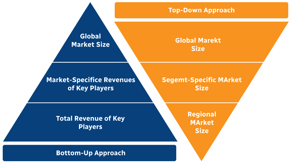
Note*: In applicable scenarios
Step 3 - Data Sources
Primary Research
- Web Analytics
- Survey Reports
- Research Institute
- Latest Research Reports
- Opinion Leaders
Secondary Research
- Annual Reports
- White Paper
- Latest Press Release
- Industry Association
- Paid Database
- Investor Presentations

Step 4 - Data Triangulation
Involves using different sources of information in order to increase the validity of a study
These sources are likely to be stakeholders in a program - participants, other researchers, program staff, other community members, and so on.
Then we put all data in single framework & apply various statistical tools to find out the dynamic on the market.
During the analysis stage, feedback from the stakeholder groups would be compared to determine areas of agreement as well as areas of divergence