

Key Insights
The global Chemical Mechanical Polishing (CMP) Pad Market is experiencing robust growth, projected to reach a significant market size in the coming years. Driven by the insatiable demand for advanced semiconductor devices across consumer electronics, automotive, and telecommunications sectors, the market is set to expand considerably. The increasing complexity of integrated circuits and the continuous miniaturization of transistors necessitate highly precise and defect-free wafer surfaces, placing CMP pads at the forefront of semiconductor manufacturing innovation. Technological advancements, such as the development of novel pad materials with superior polishing characteristics and enhanced durability, are key drivers. Furthermore, the burgeoning growth in artificial intelligence, 5G infrastructure, and the Internet of Things (IoT) are fueling the production of more sophisticated chips, directly translating into higher consumption of CMP pads. The market's trajectory is also influenced by investments in next-generation semiconductor fabrication facilities, particularly in Asia-Pacific, which is emerging as a dominant hub for chip manufacturing.
-Pad-Market.png)
Chemical Mechanical Polishing (CMP) Pad Market Market Size (In Billion)
The market's impressive trajectory, however, is not without its challenges. The high cost associated with advanced CMP pad materials and the stringent quality control required throughout the manufacturing process can act as restraints. Additionally, the reliance on a specialized supply chain and the potential for geopolitical trade disputes impacting material availability could pose hurdles. Despite these, the dominant CAGR of 7.90% underscores the market's resilience and the critical role CMP pads play in the semiconductor ecosystem. The shift towards larger wafer sizes, particularly 300 mm, is a significant trend, enabling greater manufacturing efficiency and higher wafer throughput, thus driving demand for compatible CMP pads. Key players are actively engaged in research and development to offer tailored solutions for various polishing applications and wafer technologies, further solidifying the market's expansion.
-Pad-Market.png)
Chemical Mechanical Polishing (CMP) Pad Market Company Market Share
This in-depth report provides a definitive analysis of the global Chemical Mechanical Polishing (CMP) Pad Market, encompassing market dynamics, growth trends, regional dominance, product landscape, key drivers, challenges, opportunities, and a detailed company and milestone overview. Leveraging advanced analytical frameworks and extensive data from the historical period (2019-2024), base year (2025), and forecast period (2025-2033), this report offers actionable insights for stakeholders in the semiconductor manufacturing industry, advanced materials sector, and consumable chemicals market.
Chemical Mechanical Polishing (CMP) Pad Market Market Dynamics & Structure
The Chemical Mechanical Polishing (CMP) Pad Market exhibits a moderate to high level of concentration, driven by the technological sophistication and capital investment required for pad manufacturing. Key players like 3M Co, DuPont de Nemours Inc, Fujibo Holdings Inc, Pureon, SK enpulse, Thomas West Inc, Hubei DingLong, Cabot Corporation, Entegris, and Beijing Grish Hitech Co Lt invest heavily in research and development to enhance pad performance, including achieving superior planarity, reduced defects, and extended pad life. Technological innovation is the primary driver, with continuous advancements in polymer science and surface engineering enabling the development of pads for increasingly complex 300 mm wafer polishing applications. Regulatory frameworks, particularly those concerning environmental sustainability and waste management, are gaining prominence, influencing material choices and pad recycling initiatives. Competitive product substitutes, while limited in the direct CMP pad arena, can emerge from advancements in alternative polishing techniques or slurry formulations that necessitate modified pad characteristics. End-user demographics are primarily large-scale semiconductor fabrication facilities (fabs) with stringent quality control requirements. Mergers and acquisitions (M&A) trends, as exemplified by SKC Ltd's integration with SK enpulse, indicate consolidation efforts aimed at expanding product portfolios and geographical reach within the semiconductor materials market. Barriers to entry are significant due to proprietary technologies and established customer relationships.
- Market Concentration: Moderate to High, dominated by a few key global players.
- Technological Innovation Drivers: Need for higher precision, defect reduction, and longer pad life in advanced semiconductor nodes.
- Regulatory Frameworks: Increasing focus on environmental impact and sustainable manufacturing practices.
- End-User Demographics: Predominantly large semiconductor manufacturers and foundries.
- M&A Trends: Strategic consolidation to gain market share and expand capabilities.
Chemical Mechanical Polishing (CMP) Pad Market Growth Trends & Insights
The Chemical Mechanical Polishing (CMP) Pad Market is projected for robust growth, fueled by the insatiable demand for advanced semiconductor devices across various industries. The global market size is anticipated to witness a Compound Annual Growth Rate (CAGR) of approximately 6.8% during the forecast period (2025-2033). This growth is underpinned by the increasing adoption of CMP technology in the fabrication of integrated circuits (ICs), logic devices, and memory chips. The shift towards 300 mm wafer sizes, which represent a significant portion of the market share, continues to drive the need for high-performance CMP pads capable of handling larger substrate diameters with greater uniformity. Technological disruptions, such as the development of novel pad materials with enhanced durability and reduced friction, are crucial in meeting the stringent requirements of next-generation semiconductor manufacturing processes. Consumer behavior shifts are indirectly influencing the market, as the escalating demand for consumer electronics, artificial intelligence (AI) applications, and the Internet of Things (IoT) devices necessitates a continuous expansion of semiconductor production capacity, thereby driving CMP pad consumption. Market penetration of specialized CMP pads for advanced materials like GaN and SiC is also on the rise, indicating a broadening application scope. The increasing complexity of chip architectures and the drive for smaller, more powerful transistors necessitate ongoing innovation in CMP consumables, including pads and slurries, to achieve optimal polishing results. The report will detail the evolution of market size in million units from the historical period through the forecast period, providing granular insights into this upward trajectory.
Dominant Regions, Countries, or Segments in Chemical Mechanical Polishing (CMP) Pad Market
The 300 mm wafer segment unequivocally leads the Chemical Mechanical Polishing (CMP) Pad Market, driven by its dominance in advanced semiconductor fabrication. The increasing investment in cutting-edge foundries and the production of high-performance processors, memory chips, and AI accelerators predominantly utilize 300 mm wafers. This segment alone accounts for an estimated 75% of the global CMP pad market share. The concentration of leading semiconductor manufacturers in regions like Asia-Pacific, particularly Taiwan, South Korea, and China, further solidifies the dominance of the 300 mm segment. Economic policies in these regions, often characterized by substantial government incentives for the semiconductor industry, coupled with massive infrastructure development for wafer fabs, create an environment conducive to high CMP pad consumption.
The 200 mm wafer segment, while mature, continues to represent a significant portion of the market, catering to the production of less advanced but still critical semiconductor components for automotive, industrial, and consumer electronics applications. Its market share is estimated to be around 20%. Countries like the United States and European nations maintain a strong presence in the 200 mm wafer manufacturing landscape, ensuring sustained demand for CMP pads.
The "Other Wafer Sizes" segment, including smaller diameter wafers and emerging substrates like flexible and transparent wafers, holds a smaller but growing market share of approximately 5%. This segment is driven by niche applications in specialized sensors, micro-electromechanical systems (MEMS), and emerging display technologies. Continued research and development in novel semiconductor materials and form factors will be crucial for the expansion of this segment.
Key drivers for the dominance of the 300 mm segment include:
- Economies of Scale: Larger wafer sizes enable more efficient chip production, reducing per-die costs.
- Technological Advancement: The latest and most complex ICs are manufactured on 300 mm wafers.
- Capital Investment: Significant investments in 300 mm fabs by major semiconductor players worldwide.
- Geographical Concentration: A high concentration of 300 mm fab capacity in Asia-Pacific.
Chemical Mechanical Polishing (CMP) Pad Market Product Landscape
The Chemical Mechanical Polishing (CMP) Pad Market is characterized by continuous product innovation focused on enhancing polishing efficiency, defect reduction, and extended pad life. Manufacturers are developing advanced polymer formulations and surface textures to cater to specific polishing applications, such as shallow trench isolation (STI), metal layers, and dielectric planarization. Innovations include multi-layer pads with optimized stiffness and porosity, as well as pads with improved chemical resistance and thermal management capabilities. The trend towards finer feature sizes in semiconductor manufacturing necessitates CMP pads that can achieve sub-nanometer surface roughness and minimize defects, including scratches and colloidal silica residues. Performance metrics such as removal rate, uniformity, defect density, and pad wear rate are critical differentiators.
Key Drivers, Barriers & Challenges in Chemical Mechanical Polishing (CMP) Pad Market
The Chemical Mechanical Polishing (CMP) Pad Market is propelled by several key drivers. The exponential growth in demand for semiconductors across AI, 5G, IoT, and automotive sectors directly translates to increased wafer production, thereby driving CMP pad consumption. Technological advancements in chip design, requiring higher precision and defect-free surfaces, necessitate the use of advanced CMP pads. Furthermore, the transition to next-generation wafer sizes like 300 mm and the exploration of novel semiconductor materials such as SiC and GaN are creating new opportunities for specialized CMP pad development.
Key challenges and restraints include the high capital expenditure required for establishing advanced CMP pad manufacturing facilities, coupled with the stringent quality control and proprietary technologies involved. Supply chain disruptions, as witnessed in recent global events, can impact the availability and cost of raw materials essential for pad production. Intense competition among established players and emerging manufacturers can exert downward pressure on pricing, impacting profit margins. Moreover, the environmental impact of consumable materials in semiconductor manufacturing and the increasing focus on sustainable disposal or recycling methods present both a challenge and an opportunity for innovation. The complex and lengthy qualification processes by semiconductor manufacturers for new CMP pad suppliers also pose a significant barrier.
Emerging Opportunities in Chemical Mechanical Polishing (CMP) Pad Market
Emerging opportunities in the Chemical Mechanical Polishing (CMP) Pad Market are largely driven by the relentless pace of technological evolution in the semiconductor industry and a growing emphasis on sustainability. The expansion of advanced packaging technologies, such as 3D stacking and heterogeneous integration, demands novel CMP solutions for interconnections and wafer thinning, creating a niche for specialized pads. The burgeoning market for power semiconductors, particularly those based on Silicon Carbide (SiC) and Gallium Nitride (GaN), requires CMP pads with enhanced durability and chemical resistance to handle these harder and more complex materials, representing a significant growth avenue. Furthermore, the development of eco-friendly CMP pads, including those made from recycled materials or designed for easier recycling, presents a substantial opportunity as semiconductor manufacturers increasingly prioritize environmental, social, and governance (ESG) factors. Innovations in smart manufacturing and Industry 4.0 are also creating opportunities for pads with integrated sensors or data-reporting capabilities.
Growth Accelerators in the Chemical Mechanical Polishing (CMP) Pad Market Industry
Long-term growth in the Chemical Mechanical Polishing (CMP) Pad Market is being accelerated by several factors. The continuous drive for miniaturization and increased performance in semiconductor devices, as dictated by Moore's Law and its successors, mandates ongoing advancements in CMP processes and consumables. Strategic partnerships between CMP pad manufacturers and slurry suppliers, along with collaborations with leading semiconductor fabs, are crucial for co-developing optimized polishing solutions that meet evolving process requirements. The expansion of semiconductor manufacturing capacity, particularly in emerging markets and the establishment of new fabs, directly fuels the demand for CMP pads. Furthermore, the increasing adoption of CMP in new applications beyond traditional microelectronics, such as in the manufacturing of advanced displays and MEMS devices, broadens the market scope. The development of advanced materials and novel manufacturing techniques for CMP pads that offer superior performance and cost-effectiveness will serve as significant growth catalysts.
Key Players Shaping the Chemical Mechanical Polishing (CMP) Pad Market Market
- 3M Co
- DuPont de Nemours Inc
- Fujibo Holdings Inc
- Pureon
- SK enpulse
- Thomas West Inc
- Hubei DingLong
- Cabot Corporation
- Entegris
- Beijing Grish Hitech Co Lt
Notable Milestones in Chemical Mechanical Polishing (CMP) Pad Market Sector
- December 2023: SK Hynix developed a technology for recycling chemical mechanical polishing (CMP) pads used in wafer polishing. This innovation addresses the significant cost and environmental implications associated with discarding these essential semiconductor production consumables, highlighting a growing trend towards sustainability in the industry.
- September 2023: SK enpulse Co., a key player in semiconductor materials, announced the divestment of its chip pre-manufacturing processing units in China. This move, coupled with the merger of SKC Ltd's chip materials business with SK enpulse, signifies strategic consolidation and a continued focus on promoting the chip pre-manufacturing process materials business, including chemical mechanical polishing pads, under the SK Group umbrella.
In-Depth Chemical Mechanical Polishing (CMP) Pad Market Market Outlook
The outlook for the Chemical Mechanical Polishing (CMP) Pad Market remains exceptionally strong, driven by an interconnected ecosystem of technological innovation and burgeoning demand for advanced electronics. Future growth will be significantly influenced by the increasing complexity of chip architectures and the relentless pursuit of higher processing power and energy efficiency across sectors like AI, automotive, and telecommunications. The ongoing transition to next-generation wafer sizes and the expanding applications of compound semiconductors will continue to fuel the need for high-performance, specialized CMP pads. Strategic investments in R&D, coupled with the exploration of sustainable material solutions and advanced manufacturing processes, will be critical for market leaders to maintain their competitive edge. The market is poised for sustained expansion, offering lucrative opportunities for companies that can effectively address the evolving technical demands and environmental considerations of the global semiconductor industry.
Chemical Mechanical Polishing (CMP) Pad Market Segmentation
-
1. Wafer Size
- 1.1. 300 mm
- 1.2. 200 mm
- 1.3. Other Wafer Sizes
Chemical Mechanical Polishing (CMP) Pad Market Segmentation By Geography
- 1. North America
- 2. Europe
- 3. China
- 4. South Korea
- 5. Japan
- 6. Taiwan
-Pad-Market.png)
Chemical Mechanical Polishing (CMP) Pad Market Regional Market Share
Geographic Coverage of Chemical Mechanical Polishing (CMP) Pad Market
Chemical Mechanical Polishing (CMP) Pad Market REPORT HIGHLIGHTS
| Aspects | Details |
|---|---|
| Study Period | 2020-2034 |
| Base Year | 2025 |
| Estimated Year | 2026 |
| Forecast Period | 2026-2034 |
| Historical Period | 2020-2025 |
| Growth Rate | CAGR of 7.90% from 2020-2034 |
| Segmentation |
|
Table of Contents
- 1. Introduction
- 1.1. Research Scope
- 1.2. Market Segmentation
- 1.3. Research Objective
- 1.4. Definitions and Assumptions
- 2. Executive Summary
- 2.1. Market Snapshot
- 3. Market Dynamics
- 3.1. Market Drivers
- 3.2. Market Restrains
- 3.3. Market Trends
- 3.4. Market Opportunities
- 4. Market Factor Analysis
- 4.1. Porters Five Forces
- 4.1.1. Bargaining Power of Suppliers
- 4.1.2. Bargaining Power of Buyers
- 4.1.3. Threat of New Entrants
- 4.1.4. Threat of Substitutes
- 4.1.5. Competitive Rivalry
- 4.2. PESTEL analysis
- 4.3. BCG Analysis
- 4.3.1. Stars (High Growth, High Market Share)
- 4.3.2. Cash Cows (Low Growth, High Market Share)
- 4.3.3. Question Mark (High Growth, Low Market Share)
- 4.3.4. Dogs (Low Growth, Low Market Share)
- 4.4. Ansoff Matrix Analysis
- 4.5. Supply Chain Analysis
- 4.6. Regulatory Landscape
- 4.7. Current Market Potential and Opportunity Assessment (TAM–SAM–SOM Framework)
- 4.8. VDR Analyst Note
- 4.1. Porters Five Forces
- 5. Market Analysis, Insights and Forecast 2021-2033
- 5.1. Market Analysis, Insights and Forecast - by Wafer Size
- 5.1.1. 300 mm
- 5.1.2. 200 mm
- 5.1.3. Other Wafer Sizes
- 5.2. Market Analysis, Insights and Forecast - by Region
- 5.2.1. North America
- 5.2.2. Europe
- 5.2.3. China
- 5.2.4. South Korea
- 5.2.5. Japan
- 5.2.6. Taiwan
- 5.1. Market Analysis, Insights and Forecast - by Wafer Size
- 6. Global Chemical Mechanical Polishing (CMP) Pad Market Analysis, Insights and Forecast, 2021-2033
- 6.1. Market Analysis, Insights and Forecast - by Wafer Size
- 6.1.1. 300 mm
- 6.1.2. 200 mm
- 6.1.3. Other Wafer Sizes
- 6.1. Market Analysis, Insights and Forecast - by Wafer Size
- 7. North America Chemical Mechanical Polishing (CMP) Pad Market Analysis, Insights and Forecast, 2021-2033
- 7.1. Market Analysis, Insights and Forecast - by Wafer Size
- 7.1.1. 300 mm
- 7.1.2. 200 mm
- 7.1.3. Other Wafer Sizes
- 7.1. Market Analysis, Insights and Forecast - by Wafer Size
- 8. Europe Chemical Mechanical Polishing (CMP) Pad Market Analysis, Insights and Forecast, 2021-2033
- 8.1. Market Analysis, Insights and Forecast - by Wafer Size
- 8.1.1. 300 mm
- 8.1.2. 200 mm
- 8.1.3. Other Wafer Sizes
- 8.1. Market Analysis, Insights and Forecast - by Wafer Size
- 9. China Chemical Mechanical Polishing (CMP) Pad Market Analysis, Insights and Forecast, 2021-2033
- 9.1. Market Analysis, Insights and Forecast - by Wafer Size
- 9.1.1. 300 mm
- 9.1.2. 200 mm
- 9.1.3. Other Wafer Sizes
- 9.1. Market Analysis, Insights and Forecast - by Wafer Size
- 10. South Korea Chemical Mechanical Polishing (CMP) Pad Market Analysis, Insights and Forecast, 2021-2033
- 10.1. Market Analysis, Insights and Forecast - by Wafer Size
- 10.1.1. 300 mm
- 10.1.2. 200 mm
- 10.1.3. Other Wafer Sizes
- 10.1. Market Analysis, Insights and Forecast - by Wafer Size
- 11. Japan Chemical Mechanical Polishing (CMP) Pad Market Analysis, Insights and Forecast, 2021-2033
- 11.1. Market Analysis, Insights and Forecast - by Wafer Size
- 11.1.1. 300 mm
- 11.1.2. 200 mm
- 11.1.3. Other Wafer Sizes
- 11.1. Market Analysis, Insights and Forecast - by Wafer Size
- 12. Taiwan Chemical Mechanical Polishing (CMP) Pad Market Analysis, Insights and Forecast, 2021-2033
- 12.1. Market Analysis, Insights and Forecast - by Wafer Size
- 12.1.1. 300 mm
- 12.1.2. 200 mm
- 12.1.3. Other Wafer Sizes
- 12.1. Market Analysis, Insights and Forecast - by Wafer Size
- 13. Competitive Analysis
- 13.1. Company Profiles
- 13.1.1 3M Co
- 13.1.1.1. Company Overview
- 13.1.1.2. Products
- 13.1.1.3. Company Financials
- 13.1.1.4. SWOT Analysis
- 13.1.2 DuPont de Nemours Inc
- 13.1.2.1. Company Overview
- 13.1.2.2. Products
- 13.1.2.3. Company Financials
- 13.1.2.4. SWOT Analysis
- 13.1.3 Fujibo Holdings Inc
- 13.1.3.1. Company Overview
- 13.1.3.2. Products
- 13.1.3.3. Company Financials
- 13.1.3.4. SWOT Analysis
- 13.1.4 Pureon
- 13.1.4.1. Company Overview
- 13.1.4.2. Products
- 13.1.4.3. Company Financials
- 13.1.4.4. SWOT Analysis
- 13.1.5 SK enpulse
- 13.1.5.1. Company Overview
- 13.1.5.2. Products
- 13.1.5.3. Company Financials
- 13.1.5.4. SWOT Analysis
- 13.1.6 Thomas West Inc
- 13.1.6.1. Company Overview
- 13.1.6.2. Products
- 13.1.6.3. Company Financials
- 13.1.6.4. SWOT Analysis
- 13.1.7 Hubei DingLong
- 13.1.7.1. Company Overview
- 13.1.7.2. Products
- 13.1.7.3. Company Financials
- 13.1.7.4. SWOT Analysis
- 13.1.8 Cabot Corporation
- 13.1.8.1. Company Overview
- 13.1.8.2. Products
- 13.1.8.3. Company Financials
- 13.1.8.4. SWOT Analysis
- 13.1.9 Entegris
- 13.1.9.1. Company Overview
- 13.1.9.2. Products
- 13.1.9.3. Company Financials
- 13.1.9.4. SWOT Analysis
- 13.1.10 Beijing Grish Hitech Co Lt
- 13.1.10.1. Company Overview
- 13.1.10.2. Products
- 13.1.10.3. Company Financials
- 13.1.10.4. SWOT Analysis
- 13.1.1 3M Co
- 13.2. Market Entropy
- 13.2.1 Company's Key Areas Served
- 13.2.2 Recent Developments
- 13.3. Company Market Share Analysis 2025
- 13.3.1 Top 5 Companies Market Share Analysis
- 13.3.2 Top 3 Companies Market Share Analysis
- 13.4. List of Potential Customers
- 14. Research Methodology
List of Figures
- Figure 1: Global Chemical Mechanical Polishing (CMP) Pad Market Revenue Breakdown (Million, %) by Region 2025 & 2033
- Figure 2: Global Chemical Mechanical Polishing (CMP) Pad Market Volume Breakdown (Billion, %) by Region 2025 & 2033
- Figure 3: North America Chemical Mechanical Polishing (CMP) Pad Market Revenue (Million), by Wafer Size 2025 & 2033
- Figure 4: North America Chemical Mechanical Polishing (CMP) Pad Market Volume (Billion), by Wafer Size 2025 & 2033
- Figure 5: North America Chemical Mechanical Polishing (CMP) Pad Market Revenue Share (%), by Wafer Size 2025 & 2033
- Figure 6: North America Chemical Mechanical Polishing (CMP) Pad Market Volume Share (%), by Wafer Size 2025 & 2033
- Figure 7: North America Chemical Mechanical Polishing (CMP) Pad Market Revenue (Million), by Country 2025 & 2033
- Figure 8: North America Chemical Mechanical Polishing (CMP) Pad Market Volume (Billion), by Country 2025 & 2033
- Figure 9: North America Chemical Mechanical Polishing (CMP) Pad Market Revenue Share (%), by Country 2025 & 2033
- Figure 10: North America Chemical Mechanical Polishing (CMP) Pad Market Volume Share (%), by Country 2025 & 2033
- Figure 11: Europe Chemical Mechanical Polishing (CMP) Pad Market Revenue (Million), by Wafer Size 2025 & 2033
- Figure 12: Europe Chemical Mechanical Polishing (CMP) Pad Market Volume (Billion), by Wafer Size 2025 & 2033
- Figure 13: Europe Chemical Mechanical Polishing (CMP) Pad Market Revenue Share (%), by Wafer Size 2025 & 2033
- Figure 14: Europe Chemical Mechanical Polishing (CMP) Pad Market Volume Share (%), by Wafer Size 2025 & 2033
- Figure 15: Europe Chemical Mechanical Polishing (CMP) Pad Market Revenue (Million), by Country 2025 & 2033
- Figure 16: Europe Chemical Mechanical Polishing (CMP) Pad Market Volume (Billion), by Country 2025 & 2033
- Figure 17: Europe Chemical Mechanical Polishing (CMP) Pad Market Revenue Share (%), by Country 2025 & 2033
- Figure 18: Europe Chemical Mechanical Polishing (CMP) Pad Market Volume Share (%), by Country 2025 & 2033
- Figure 19: China Chemical Mechanical Polishing (CMP) Pad Market Revenue (Million), by Wafer Size 2025 & 2033
- Figure 20: China Chemical Mechanical Polishing (CMP) Pad Market Volume (Billion), by Wafer Size 2025 & 2033
- Figure 21: China Chemical Mechanical Polishing (CMP) Pad Market Revenue Share (%), by Wafer Size 2025 & 2033
- Figure 22: China Chemical Mechanical Polishing (CMP) Pad Market Volume Share (%), by Wafer Size 2025 & 2033
- Figure 23: China Chemical Mechanical Polishing (CMP) Pad Market Revenue (Million), by Country 2025 & 2033
- Figure 24: China Chemical Mechanical Polishing (CMP) Pad Market Volume (Billion), by Country 2025 & 2033
- Figure 25: China Chemical Mechanical Polishing (CMP) Pad Market Revenue Share (%), by Country 2025 & 2033
- Figure 26: China Chemical Mechanical Polishing (CMP) Pad Market Volume Share (%), by Country 2025 & 2033
- Figure 27: South Korea Chemical Mechanical Polishing (CMP) Pad Market Revenue (Million), by Wafer Size 2025 & 2033
- Figure 28: South Korea Chemical Mechanical Polishing (CMP) Pad Market Volume (Billion), by Wafer Size 2025 & 2033
- Figure 29: South Korea Chemical Mechanical Polishing (CMP) Pad Market Revenue Share (%), by Wafer Size 2025 & 2033
- Figure 30: South Korea Chemical Mechanical Polishing (CMP) Pad Market Volume Share (%), by Wafer Size 2025 & 2033
- Figure 31: South Korea Chemical Mechanical Polishing (CMP) Pad Market Revenue (Million), by Country 2025 & 2033
- Figure 32: South Korea Chemical Mechanical Polishing (CMP) Pad Market Volume (Billion), by Country 2025 & 2033
- Figure 33: South Korea Chemical Mechanical Polishing (CMP) Pad Market Revenue Share (%), by Country 2025 & 2033
- Figure 34: South Korea Chemical Mechanical Polishing (CMP) Pad Market Volume Share (%), by Country 2025 & 2033
- Figure 35: Japan Chemical Mechanical Polishing (CMP) Pad Market Revenue (Million), by Wafer Size 2025 & 2033
- Figure 36: Japan Chemical Mechanical Polishing (CMP) Pad Market Volume (Billion), by Wafer Size 2025 & 2033
- Figure 37: Japan Chemical Mechanical Polishing (CMP) Pad Market Revenue Share (%), by Wafer Size 2025 & 2033
- Figure 38: Japan Chemical Mechanical Polishing (CMP) Pad Market Volume Share (%), by Wafer Size 2025 & 2033
- Figure 39: Japan Chemical Mechanical Polishing (CMP) Pad Market Revenue (Million), by Country 2025 & 2033
- Figure 40: Japan Chemical Mechanical Polishing (CMP) Pad Market Volume (Billion), by Country 2025 & 2033
- Figure 41: Japan Chemical Mechanical Polishing (CMP) Pad Market Revenue Share (%), by Country 2025 & 2033
- Figure 42: Japan Chemical Mechanical Polishing (CMP) Pad Market Volume Share (%), by Country 2025 & 2033
- Figure 43: Taiwan Chemical Mechanical Polishing (CMP) Pad Market Revenue (Million), by Wafer Size 2025 & 2033
- Figure 44: Taiwan Chemical Mechanical Polishing (CMP) Pad Market Volume (Billion), by Wafer Size 2025 & 2033
- Figure 45: Taiwan Chemical Mechanical Polishing (CMP) Pad Market Revenue Share (%), by Wafer Size 2025 & 2033
- Figure 46: Taiwan Chemical Mechanical Polishing (CMP) Pad Market Volume Share (%), by Wafer Size 2025 & 2033
- Figure 47: Taiwan Chemical Mechanical Polishing (CMP) Pad Market Revenue (Million), by Country 2025 & 2033
- Figure 48: Taiwan Chemical Mechanical Polishing (CMP) Pad Market Volume (Billion), by Country 2025 & 2033
- Figure 49: Taiwan Chemical Mechanical Polishing (CMP) Pad Market Revenue Share (%), by Country 2025 & 2033
- Figure 50: Taiwan Chemical Mechanical Polishing (CMP) Pad Market Volume Share (%), by Country 2025 & 2033
List of Tables
- Table 1: Global Chemical Mechanical Polishing (CMP) Pad Market Revenue Million Forecast, by Wafer Size 2020 & 2033
- Table 2: Global Chemical Mechanical Polishing (CMP) Pad Market Volume Billion Forecast, by Wafer Size 2020 & 2033
- Table 3: Global Chemical Mechanical Polishing (CMP) Pad Market Revenue Million Forecast, by Region 2020 & 2033
- Table 4: Global Chemical Mechanical Polishing (CMP) Pad Market Volume Billion Forecast, by Region 2020 & 2033
- Table 5: Global Chemical Mechanical Polishing (CMP) Pad Market Revenue Million Forecast, by Wafer Size 2020 & 2033
- Table 6: Global Chemical Mechanical Polishing (CMP) Pad Market Volume Billion Forecast, by Wafer Size 2020 & 2033
- Table 7: Global Chemical Mechanical Polishing (CMP) Pad Market Revenue Million Forecast, by Country 2020 & 2033
- Table 8: Global Chemical Mechanical Polishing (CMP) Pad Market Volume Billion Forecast, by Country 2020 & 2033
- Table 9: Global Chemical Mechanical Polishing (CMP) Pad Market Revenue Million Forecast, by Wafer Size 2020 & 2033
- Table 10: Global Chemical Mechanical Polishing (CMP) Pad Market Volume Billion Forecast, by Wafer Size 2020 & 2033
- Table 11: Global Chemical Mechanical Polishing (CMP) Pad Market Revenue Million Forecast, by Country 2020 & 2033
- Table 12: Global Chemical Mechanical Polishing (CMP) Pad Market Volume Billion Forecast, by Country 2020 & 2033
- Table 13: Global Chemical Mechanical Polishing (CMP) Pad Market Revenue Million Forecast, by Wafer Size 2020 & 2033
- Table 14: Global Chemical Mechanical Polishing (CMP) Pad Market Volume Billion Forecast, by Wafer Size 2020 & 2033
- Table 15: Global Chemical Mechanical Polishing (CMP) Pad Market Revenue Million Forecast, by Country 2020 & 2033
- Table 16: Global Chemical Mechanical Polishing (CMP) Pad Market Volume Billion Forecast, by Country 2020 & 2033
- Table 17: Global Chemical Mechanical Polishing (CMP) Pad Market Revenue Million Forecast, by Wafer Size 2020 & 2033
- Table 18: Global Chemical Mechanical Polishing (CMP) Pad Market Volume Billion Forecast, by Wafer Size 2020 & 2033
- Table 19: Global Chemical Mechanical Polishing (CMP) Pad Market Revenue Million Forecast, by Country 2020 & 2033
- Table 20: Global Chemical Mechanical Polishing (CMP) Pad Market Volume Billion Forecast, by Country 2020 & 2033
- Table 21: Global Chemical Mechanical Polishing (CMP) Pad Market Revenue Million Forecast, by Wafer Size 2020 & 2033
- Table 22: Global Chemical Mechanical Polishing (CMP) Pad Market Volume Billion Forecast, by Wafer Size 2020 & 2033
- Table 23: Global Chemical Mechanical Polishing (CMP) Pad Market Revenue Million Forecast, by Country 2020 & 2033
- Table 24: Global Chemical Mechanical Polishing (CMP) Pad Market Volume Billion Forecast, by Country 2020 & 2033
- Table 25: Global Chemical Mechanical Polishing (CMP) Pad Market Revenue Million Forecast, by Wafer Size 2020 & 2033
- Table 26: Global Chemical Mechanical Polishing (CMP) Pad Market Volume Billion Forecast, by Wafer Size 2020 & 2033
- Table 27: Global Chemical Mechanical Polishing (CMP) Pad Market Revenue Million Forecast, by Country 2020 & 2033
- Table 28: Global Chemical Mechanical Polishing (CMP) Pad Market Volume Billion Forecast, by Country 2020 & 2033
Frequently Asked Questions
1. What is the projected Compound Annual Growth Rate (CAGR) of the Chemical Mechanical Polishing (CMP) Pad Market?
The projected CAGR is approximately 7.90%.
2. Which companies are prominent players in the Chemical Mechanical Polishing (CMP) Pad Market?
Key companies in the market include 3M Co, DuPont de Nemours Inc, Fujibo Holdings Inc, Pureon, SK enpulse, Thomas West Inc, Hubei DingLong, Cabot Corporation, Entegris, Beijing Grish Hitech Co Lt.
3. What are the main segments of the Chemical Mechanical Polishing (CMP) Pad Market?
The market segments include Wafer Size.
4. Can you provide details about the market size?
The market size is estimated to be USD 4 Million as of 2022.
5. What are some drivers contributing to market growth?
Increasing Need for Complex and High-Performance Chips/Advanced Technologies; Introduction of Smaller Nodes and New Architectures.
6. What are the notable trends driving market growth?
300 mm Wafer Size to Witness a Significant Growth.
7. Are there any restraints impacting market growth?
Increasing Need for Complex and High-Performance Chips/Advanced Technologies; Introduction of Smaller Nodes and New Architectures.
8. Can you provide examples of recent developments in the market?
December 2023: Essential consumable materials used in semiconductor production, like wafers, slurries, and pads, are typically discarded at the end of the manufacturing process. Disposing of these materials not only incurs a significant cost but also has negative environmental implications due to the carbon and harmful gases. SK Hynix created a technology for recycling chemical mechanical polishing (CMP) pads used in the wafer polishing stage to address this issue.
9. What pricing options are available for accessing the report?
Pricing options include single-user, multi-user, and enterprise licenses priced at USD 4750, USD 5250, and USD 8750 respectively.
10. Is the market size provided in terms of value or volume?
The market size is provided in terms of value, measured in Million and volume, measured in Billion.
11. Are there any specific market keywords associated with the report?
Yes, the market keyword associated with the report is "Chemical Mechanical Polishing (CMP) Pad Market," which aids in identifying and referencing the specific market segment covered.
12. How do I determine which pricing option suits my needs best?
The pricing options vary based on user requirements and access needs. Individual users may opt for single-user licenses, while businesses requiring broader access may choose multi-user or enterprise licenses for cost-effective access to the report.
13. Are there any additional resources or data provided in the Chemical Mechanical Polishing (CMP) Pad Market report?
While the report offers comprehensive insights, it's advisable to review the specific contents or supplementary materials provided to ascertain if additional resources or data are available.
14. How can I stay updated on further developments or reports in the Chemical Mechanical Polishing (CMP) Pad Market?
To stay informed about further developments, trends, and reports in the Chemical Mechanical Polishing (CMP) Pad Market, consider subscribing to industry newsletters, following relevant companies and organizations, or regularly checking reputable industry news sources and publications.
Methodology
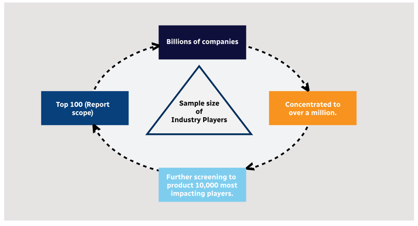
Step 1 - Identification of Relevant Samples Size from Population Database


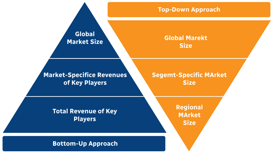
Step 2 - Approaches for Defining Global Market Size (Value, Volume* & Price*)
Note*: In applicable scenarios
Step 3 - Data Sources
Primary Research
- Web Analytics
- Survey Reports
- Research Institute
- Latest Research Reports
- Opinion Leaders
Secondary Research
- Annual Reports
- White Paper
- Latest Press Release
- Industry Association
- Paid Database
- Investor Presentations

Step 4 - Data Triangulation
Involves using different sources of information in order to increase the validity of a study
These sources are likely to be stakeholders in a program - participants, other researchers, program staff, other community members, and so on.
Then we put all data in single framework & apply various statistical tools to find out the dynamic on the market.
During the analysis stage, feedback from the stakeholder groups would be compared to determine areas of agreement as well as areas of divergence