

Key Insights
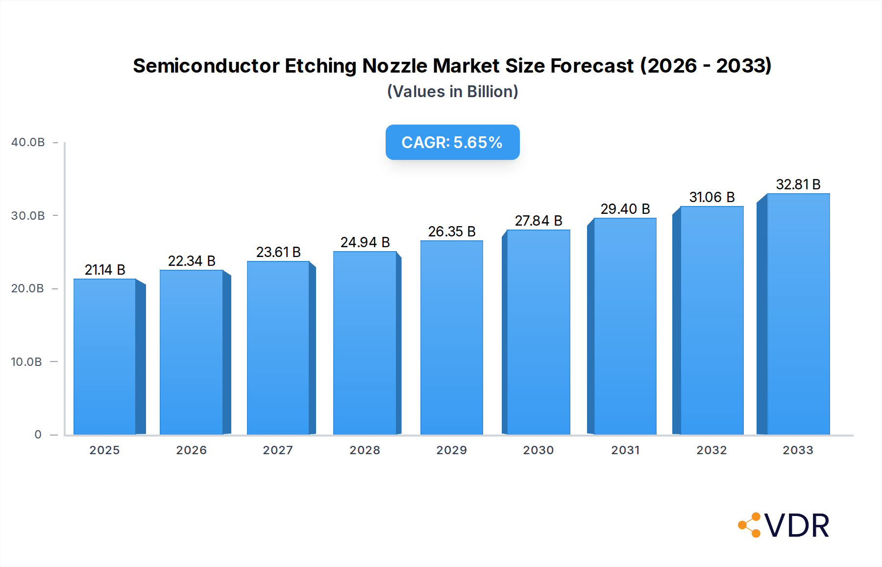
The global Semiconductor Etching Nozzle market is poised for significant expansion, projected to reach an estimated USD 21,140 million in 2025. This robust growth is underpinned by a compelling Compound Annual Growth Rate (CAGR) of 5.7%, indicating sustained momentum throughout the forecast period of 2025-2033. The primary impetus for this upward trajectory stems from the escalating demand for advanced semiconductor devices across a multitude of critical industries. The burgeoning automotive sector, driven by the proliferation of electric vehicles and sophisticated driver-assistance systems, requires increasingly complex and high-performance integrated circuits, directly boosting the need for precision etching components. Similarly, the solar cell industry's rapid advancement and the consistent demand for cutting-edge consumer electronics, from smartphones to AI-powered devices, are significant growth catalysts. The evolution of manufacturing processes within these sectors necessitates higher precision and efficiency in etching technologies, positioning semiconductor etching nozzles as indispensable components.

Semiconductor Etching Nozzle Market Size (In Billion)
Further fueling this market's ascent are key technological advancements and evolving industry trends. The relentless pursuit of smaller, more powerful, and energy-efficient chips by semiconductor manufacturers is driving innovation in etching nozzle design, emphasizing improved material deposition, enhanced etch uniformity, and greater process control. The increasing complexity of wafer fabrication, particularly with the advent of advanced packaging technologies, demands specialized etching solutions. While the market benefits from these strong drivers, it also faces certain considerations. The high capital expenditure required for advanced semiconductor manufacturing equipment, including precision etching systems, can present a barrier to entry for smaller players. Furthermore, fluctuations in the supply chain for raw materials and the intense competition among established and emerging players contribute to the market's dynamic landscape. Despite these challenges, the fundamental demand for semiconductors, coupled with ongoing technological innovation, ensures a promising outlook for the Semiconductor Etching Nozzle market.
Semiconductor Etching Nozzle Company Market Share
Semiconductor Etching Nozzle Market: A Comprehensive Outlook (2019–2033)
This in-depth report provides a granular analysis of the global Semiconductor Etching Nozzle market, offering critical insights for industry stakeholders. Covering a study period from 2019 to 2033, with a base year of 2025, this report meticulously examines market dynamics, growth trends, regional dominance, product landscape, key drivers, challenges, emerging opportunities, and the competitive ecosystem. We present quantitative data in millions of units where available or utilize predicted values for comprehensive market understanding.
Semiconductor Etching Nozzle Market Dynamics & Structure
The global semiconductor etching nozzle market exhibits a moderate level of concentration, with key players like Tokyo Electron Limited (TEL), Applied Materials, and Lam Research Corporation holding significant shares. Technological innovation is the primary driver, fueled by the relentless demand for smaller, more powerful semiconductor devices, particularly in consumer electronics and the burgeoning automotive sector. Advancements in plasma etching techniques and the development of specialized nozzles for advanced packaging solutions are at the forefront of this innovation wave. Regulatory frameworks, though generally less stringent for nozzle components themselves, are indirectly influenced by semiconductor manufacturing standards and environmental regulations concerning process gases and waste management. Competitive product substitutes are limited within the core function of precision etching nozzles, but advancements in alternative etching technologies or integrated process equipment could pose indirect threats. End-user demographics are diverse, spanning major semiconductor foundries, integrated device manufacturers (IDMs), and research institutions. Mergers and acquisitions (M&A) activity is a strategic lever for market consolidation and technology acquisition. For instance, recent years have seen several acquisitions aimed at bolstering capabilities in advanced materials and specialized nozzle designs. While specific M&A deal volumes are proprietary, the trend indicates a drive towards enhanced market share and technological synergy. Innovation barriers include the high cost of R&D for novel materials capable of withstanding extreme etching conditions and the need for ultra-precise manufacturing processes to ensure sub-micron tolerances.
- Market Concentration: Moderate, with a few dominant players.
- Technological Innovation: Driven by miniaturization and advanced packaging demands.
- Regulatory Frameworks: Indirect influence from semiconductor manufacturing standards.
- Competitive Product Substitutes: Limited for core nozzle function, but indirect threats from alternative technologies exist.
- End-User Demographics: Broad, including foundries, IDMs, and research institutions.
- M&A Trends: Strategic consolidations for market share and technology acquisition.
- Innovation Barriers: High R&D costs for advanced materials and ultra-precision manufacturing.
Semiconductor Etching Nozzle Growth Trends & Insights
The global semiconductor etching nozzle market is poised for robust growth, projected to expand significantly over the forecast period. The market size, estimated at approximately $1,500 million in the base year of 2025, is expected to witness a compound annual growth rate (CAGR) of xx% from 2025 to 2033. This expansion is intrinsically linked to the escalating demand for advanced semiconductors across multiple high-growth industries. The adoption rates of next-generation semiconductor devices, driven by the proliferation of 5G technology, artificial intelligence (AI), and the Internet of Things (IoT), are directly translating into increased demand for sophisticated etching processes and, consequently, high-performance etching nozzles. Technological disruptions, such as the shift towards 3D NAND flash memory and advanced logic chip architectures, necessitate specialized etching nozzles capable of achieving finer feature sizes and improved etch profiles. These advancements require nozzles made from advanced ceramics and polymers that can withstand aggressive plasma chemistries and high temperatures. Consumer behavior shifts, including the relentless pursuit of more powerful and energy-efficient electronic devices, are indirectly fueling this market by pushing the boundaries of semiconductor manufacturing. The increasing complexity of wafer fabrication processes requires higher precision and reliability from every component, including etching nozzles. Furthermore, the automotive industry's growing reliance on advanced electronic control units (ECUs) and autonomous driving systems, along with the solar cell industry's drive for higher efficiency, are significant contributors to the market's upward trajectory. The historical period from 2019 to 2024 laid a solid foundation, with steady growth driven by the continuous evolution of the semiconductor industry. The estimated market size for 2025 serves as a critical benchmark, reflecting current industry trends and the immediate future outlook. Market penetration is deepening as more semiconductor manufacturers invest in advanced process equipment and upgrade their existing lines to accommodate new chip designs. The focus on miniaturization, power efficiency, and enhanced performance characteristics across various end-user applications ensures a sustained demand for innovative and reliable semiconductor etching nozzles. The interplay between technological advancements, increasing semiconductor complexity, and the expanding application landscape paints a promising picture for the future of this critical component market.
Dominant Regions, Countries, or Segments in Semiconductor Etching Nozzle
The semiconductor etching nozzle market is witnessing dynamic regional and segmental growth, with certain areas and applications emerging as key drivers. Consumer Electronics stands out as a dominant segment within the application landscape, driven by the insatiable global demand for smartphones, laptops, wearables, and gaming consoles. The continuous innovation cycle in this sector necessitates frequent upgrades to semiconductor manufacturing capabilities, directly impacting the demand for advanced etching nozzles. Regions with a strong concentration of consumer electronics manufacturing, such as East Asia, particularly Taiwan, South Korea, and China, are therefore pivotal to the market's expansion. These countries are home to the world's leading foundries and assembly plants, making them prime markets for semiconductor etching nozzles.
Within the Type segmentation, Dry Etch Nozzles are experiencing accelerated growth. This is primarily attributed to the increasing adoption of plasma etching techniques for advanced semiconductor fabrication processes. Dry etching offers superior control over etch profiles, enabling the creation of intricate and high-aspect-ratio features crucial for modern chip designs. Technological advancements in plasma source design and control systems further enhance the precision and efficiency of dry etching, making dry etch nozzles indispensable.
Several key drivers underpin the dominance of these regions and segments. Economic policies in East Asian countries have historically favored the development of robust semiconductor ecosystems, including significant government investment and incentives for wafer fabrication facilities. Infrastructure development, including the availability of advanced manufacturing facilities and a skilled workforce, further bolsters their leading position. The sheer volume of semiconductor production in these regions translates into a consistently high demand for etching nozzles.
The market share for Consumer Electronics applications in the global etching nozzle market is estimated to be xx% in 2025, with a projected growth rate of xx% annually. Similarly, Dry Etch Nozzles account for approximately xx% of the total market, with an anticipated CAGR of xx% during the forecast period. The growth potential in these areas is immense, fueled by ongoing technological advancements and the expanding end-user applications of semiconductors. The continuous need for smaller, faster, and more power-efficient chips in consumer devices, coupled with the precision and control offered by dry etching, solidifies their leading roles in shaping the future of the semiconductor etching nozzle market.
Semiconductor Etching Nozzle Product Landscape
The semiconductor etching nozzle product landscape is characterized by continuous innovation focused on enhancing precision, throughput, and material compatibility. Manufacturers are developing nozzles from advanced ceramic materials, such as alumina and silicon carbide, known for their exceptional resistance to corrosive plasma chemistries and high-temperature environments. Innovations include designs that optimize gas flow dynamics, ensuring uniform etch rates across the wafer and minimizing process variations. Specialized nozzle geometries are being engineered to support advanced lithography techniques like EUV (Extreme Ultraviolet), enabling finer feature sizes and improved critical dimension control. The trend is towards modular and interchangeable nozzle designs to facilitate easier maintenance and customization for diverse etching processes, including deep reactive ion etching (DRIE) for MEMS and advanced packaging applications. Performance metrics such as etch uniformity, selectivity, and etch rate are paramount, with new products achieving industry-leading specifications.
Key Drivers, Barriers & Challenges in Semiconductor Etching Nozzle
Key Drivers: The primary forces propelling the semiconductor etching nozzle market are the relentless demand for advanced semiconductors across diverse applications, including consumer electronics, automotive, and data centers. Technological advancements in chip design, such as miniaturization and 3D architectures, necessitate more sophisticated etching processes and, consequently, higher-performance nozzles. Government initiatives supporting domestic semiconductor manufacturing and supply chain resilience also act as significant growth accelerators. The increasing complexity of wafer fabrication demands enhanced precision and reliability from all process components.
- Technological Advancements: Miniaturization, 3D chip architectures, EUV lithography.
- End-User Demand: Proliferation of AI, 5G, IoT, and advanced automotive systems.
- Government Support: Incentives for domestic semiconductor production and supply chain security.
- Process Requirements: Need for higher precision, uniformity, and selectivity in etching.
Key Challenges & Restraints: Supply chain disruptions, exacerbated by geopolitical tensions and raw material availability, pose a significant challenge. The high cost of R&D and the specialized manufacturing expertise required for advanced nozzle production also act as restraints. Stringent quality control and the need for extremely tight manufacturing tolerances contribute to high production costs. Furthermore, the long qualification cycles for new nozzle designs in the highly regulated semiconductor industry can slow down market adoption. Competitive pressures from established players and the potential for in-house development by large semiconductor manufacturers also present hurdles.
- Supply Chain Vulnerabilities: Raw material shortages, geopolitical disruptions.
- High R&D and Manufacturing Costs: Specialized materials and precision engineering.
- Stringent Quality Control: Ultra-tight tolerances and defect-free production.
- Long Qualification Cycles: Regulatory hurdles and extensive testing in semiconductor fabs.
- Competitive Pressures: Established players and potential in-house development.
Emerging Opportunities in Semiconductor Etching Nozzle
Emerging opportunities in the semiconductor etching nozzle market lie in the growing demand for specialized nozzles tailored for advanced packaging technologies, such as chiplets and heterogeneous integration. The expansion of the electric vehicle (EV) market and the increasing integration of power semiconductors present new avenues for growth. Furthermore, research into novel plasma chemistries and alternative etching techniques could unlock demand for entirely new nozzle designs and materials. Untapped markets in emerging economies with nascent semiconductor manufacturing sectors also represent significant growth potential. The development of smart nozzles with integrated sensors for real-time process monitoring and feedback control is another promising area.
Growth Accelerators in the Semiconductor Etching Nozzle Industry
The long-term growth of the semiconductor etching nozzle industry is propelled by several key catalysts. Continuous technological breakthroughs in semiconductor manufacturing processes, such as advancements in atomic layer etching (ALE) and the development of novel plasma sources, will drive the need for next-generation nozzles. Strategic partnerships between nozzle manufacturers and leading semiconductor equipment providers are crucial for co-development and faster market penetration. Market expansion strategies, including the exploration of new geographic regions and the diversification of application segments beyond traditional consumer electronics, will further fuel growth. The increasing focus on sustainability and energy efficiency in semiconductor manufacturing will also create opportunities for nozzles that contribute to reduced process gas consumption and waste.
Key Players Shaping the Semiconductor Etching Nozzle Market
- CoorsTek
- TEL (Tokyo Electron Limited)
- Samco Inc.
- MKS Instruments
- JST (Japan Solderless Terminals)
- Lam Research Corporation
- Applied Materials
- Mistec
- Hitachi High-Tech Corporation
- Mattson Technology
Notable Milestones in Semiconductor Etching Nozzle Sector
- 2019: Introduction of advanced ceramic nozzles with enhanced plasma resistance by CoorsTek.
- 2020: TEL announces advancements in dry etch nozzle technology for 3D NAND fabrication.
- 2021: Lam Research Corporation highlights innovations in plasma etch nozzles for next-generation logic devices.
- 2022: Samco Inc. showcases novel nozzle designs for improved etch uniformity in advanced packaging.
- 2023: MKS Instruments acquires a leading provider of plasma etch components, expanding its portfolio.
- 2024: Mattson Technology introduces new nozzle configurations for enhanced throughput in wafer etching.
In-Depth Semiconductor Etching Nozzle Market Outlook
The semiconductor etching nozzle market is poised for sustained and significant growth, driven by the accelerating pace of semiconductor innovation and the expanding adoption of advanced electronic devices across all sectors. Future market potential will be shaped by the industry's ability to develop and deploy ultra-precise, highly durable, and cost-effective nozzle solutions that can meet the ever-increasing demands of sub-5nm process nodes and complex 3D architectures. Strategic opportunities abound for companies that can offer customized solutions for emerging applications like advanced heterogeneous integration and specialized power device manufacturing. Continuous investment in R&D, fostering collaborations with semiconductor equipment manufacturers, and adapting to evolving supply chain dynamics will be critical for players to capitalize on the robust growth trajectory ahead.
Semiconductor Etching Nozzle Segmentation
-
1. Application
- 1.1. Automobile
- 1.2. Solar Cell
- 1.3. Consumer Electronics
- 1.4. Other
-
2. Type
- 2.1. Dry Etch Nozzles
- 2.2. Wet Etch Nozzles
Semiconductor Etching Nozzle Segmentation By Geography
-
1. North America
- 1.1. United States
- 1.2. Canada
- 1.3. Mexico
-
2. South America
- 2.1. Brazil
- 2.2. Argentina
- 2.3. Rest of South America
-
3. Europe
- 3.1. United Kingdom
- 3.2. Germany
- 3.3. France
- 3.4. Italy
- 3.5. Spain
- 3.6. Russia
- 3.7. Benelux
- 3.8. Nordics
- 3.9. Rest of Europe
-
4. Middle East & Africa
- 4.1. Turkey
- 4.2. Israel
- 4.3. GCC
- 4.4. North Africa
- 4.5. South Africa
- 4.6. Rest of Middle East & Africa
-
5. Asia Pacific
- 5.1. China
- 5.2. India
- 5.3. Japan
- 5.4. South Korea
- 5.5. ASEAN
- 5.6. Oceania
- 5.7. Rest of Asia Pacific
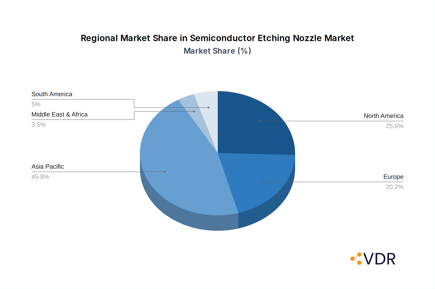
Semiconductor Etching Nozzle Regional Market Share
Geographic Coverage of Semiconductor Etching Nozzle
Semiconductor Etching Nozzle REPORT HIGHLIGHTS
| Aspects | Details |
|---|---|
| Study Period | 2020-2034 |
| Base Year | 2025 |
| Estimated Year | 2026 |
| Forecast Period | 2026-2034 |
| Historical Period | 2020-2025 |
| Growth Rate | CAGR of 5.7% from 2020-2034 |
| Segmentation |
|
Table of Contents
- 1. Introduction
- 1.1. Research Scope
- 1.2. Market Segmentation
- 1.3. Research Methodology
- 1.4. Definitions and Assumptions
- 2. Executive Summary
- 2.1. Introduction
- 3. Market Dynamics
- 3.1. Introduction
- 3.2. Market Drivers
- 3.3. Market Restrains
- 3.4. Market Trends
- 4. Market Factor Analysis
- 4.1. Porters Five Forces
- 4.2. Supply/Value Chain
- 4.3. PESTEL analysis
- 4.4. Market Entropy
- 4.5. Patent/Trademark Analysis
- 5. Global Semiconductor Etching Nozzle Analysis, Insights and Forecast, 2020-2032
- 5.1. Market Analysis, Insights and Forecast - by Application
- 5.1.1. Automobile
- 5.1.2. Solar Cell
- 5.1.3. Consumer Electronics
- 5.1.4. Other
- 5.2. Market Analysis, Insights and Forecast - by Type
- 5.2.1. Dry Etch Nozzles
- 5.2.2. Wet Etch Nozzles
- 5.3. Market Analysis, Insights and Forecast - by Region
- 5.3.1. North America
- 5.3.2. South America
- 5.3.3. Europe
- 5.3.4. Middle East & Africa
- 5.3.5. Asia Pacific
- 5.1. Market Analysis, Insights and Forecast - by Application
- 6. North America Semiconductor Etching Nozzle Analysis, Insights and Forecast, 2020-2032
- 6.1. Market Analysis, Insights and Forecast - by Application
- 6.1.1. Automobile
- 6.1.2. Solar Cell
- 6.1.3. Consumer Electronics
- 6.1.4. Other
- 6.2. Market Analysis, Insights and Forecast - by Type
- 6.2.1. Dry Etch Nozzles
- 6.2.2. Wet Etch Nozzles
- 6.1. Market Analysis, Insights and Forecast - by Application
- 7. South America Semiconductor Etching Nozzle Analysis, Insights and Forecast, 2020-2032
- 7.1. Market Analysis, Insights and Forecast - by Application
- 7.1.1. Automobile
- 7.1.2. Solar Cell
- 7.1.3. Consumer Electronics
- 7.1.4. Other
- 7.2. Market Analysis, Insights and Forecast - by Type
- 7.2.1. Dry Etch Nozzles
- 7.2.2. Wet Etch Nozzles
- 7.1. Market Analysis, Insights and Forecast - by Application
- 8. Europe Semiconductor Etching Nozzle Analysis, Insights and Forecast, 2020-2032
- 8.1. Market Analysis, Insights and Forecast - by Application
- 8.1.1. Automobile
- 8.1.2. Solar Cell
- 8.1.3. Consumer Electronics
- 8.1.4. Other
- 8.2. Market Analysis, Insights and Forecast - by Type
- 8.2.1. Dry Etch Nozzles
- 8.2.2. Wet Etch Nozzles
- 8.1. Market Analysis, Insights and Forecast - by Application
- 9. Middle East & Africa Semiconductor Etching Nozzle Analysis, Insights and Forecast, 2020-2032
- 9.1. Market Analysis, Insights and Forecast - by Application
- 9.1.1. Automobile
- 9.1.2. Solar Cell
- 9.1.3. Consumer Electronics
- 9.1.4. Other
- 9.2. Market Analysis, Insights and Forecast - by Type
- 9.2.1. Dry Etch Nozzles
- 9.2.2. Wet Etch Nozzles
- 9.1. Market Analysis, Insights and Forecast - by Application
- 10. Asia Pacific Semiconductor Etching Nozzle Analysis, Insights and Forecast, 2020-2032
- 10.1. Market Analysis, Insights and Forecast - by Application
- 10.1.1. Automobile
- 10.1.2. Solar Cell
- 10.1.3. Consumer Electronics
- 10.1.4. Other
- 10.2. Market Analysis, Insights and Forecast - by Type
- 10.2.1. Dry Etch Nozzles
- 10.2.2. Wet Etch Nozzles
- 10.1. Market Analysis, Insights and Forecast - by Application
- 11. Competitive Analysis
- 11.1. Global Market Share Analysis 2025
- 11.2. Company Profiles
- 11.2.1 CoorsTek
- 11.2.1.1. Overview
- 11.2.1.2. Products
- 11.2.1.3. SWOT Analysis
- 11.2.1.4. Recent Developments
- 11.2.1.5. Financials (Based on Availability)
- 11.2.2 TEL
- 11.2.2.1. Overview
- 11.2.2.2. Products
- 11.2.2.3. SWOT Analysis
- 11.2.2.4. Recent Developments
- 11.2.2.5. Financials (Based on Availability)
- 11.2.3 Samco
- 11.2.3.1. Overview
- 11.2.3.2. Products
- 11.2.3.3. SWOT Analysis
- 11.2.3.4. Recent Developments
- 11.2.3.5. Financials (Based on Availability)
- 11.2.4 MKS Instruments
- 11.2.4.1. Overview
- 11.2.4.2. Products
- 11.2.4.3. SWOT Analysis
- 11.2.4.4. Recent Developments
- 11.2.4.5. Financials (Based on Availability)
- 11.2.5 JST
- 11.2.5.1. Overview
- 11.2.5.2. Products
- 11.2.5.3. SWOT Analysis
- 11.2.5.4. Recent Developments
- 11.2.5.5. Financials (Based on Availability)
- 11.2.6 Lam Research Corporation
- 11.2.6.1. Overview
- 11.2.6.2. Products
- 11.2.6.3. SWOT Analysis
- 11.2.6.4. Recent Developments
- 11.2.6.5. Financials (Based on Availability)
- 11.2.7 Applied Materials
- 11.2.7.1. Overview
- 11.2.7.2. Products
- 11.2.7.3. SWOT Analysis
- 11.2.7.4. Recent Developments
- 11.2.7.5. Financials (Based on Availability)
- 11.2.8 Mistec
- 11.2.8.1. Overview
- 11.2.8.2. Products
- 11.2.8.3. SWOT Analysis
- 11.2.8.4. Recent Developments
- 11.2.8.5. Financials (Based on Availability)
- 11.2.9 Tokyo Electron Limited
- 11.2.9.1. Overview
- 11.2.9.2. Products
- 11.2.9.3. SWOT Analysis
- 11.2.9.4. Recent Developments
- 11.2.9.5. Financials (Based on Availability)
- 11.2.10 Hitachi High-Tech Corporation
- 11.2.10.1. Overview
- 11.2.10.2. Products
- 11.2.10.3. SWOT Analysis
- 11.2.10.4. Recent Developments
- 11.2.10.5. Financials (Based on Availability)
- 11.2.11 Mattson Technology
- 11.2.11.1. Overview
- 11.2.11.2. Products
- 11.2.11.3. SWOT Analysis
- 11.2.11.4. Recent Developments
- 11.2.11.5. Financials (Based on Availability)
- 11.2.1 CoorsTek
List of Figures
- Figure 1: Global Semiconductor Etching Nozzle Revenue Breakdown (undefined, %) by Region 2025 & 2033
- Figure 2: North America Semiconductor Etching Nozzle Revenue (undefined), by Application 2025 & 2033
- Figure 3: North America Semiconductor Etching Nozzle Revenue Share (%), by Application 2025 & 2033
- Figure 4: North America Semiconductor Etching Nozzle Revenue (undefined), by Type 2025 & 2033
- Figure 5: North America Semiconductor Etching Nozzle Revenue Share (%), by Type 2025 & 2033
- Figure 6: North America Semiconductor Etching Nozzle Revenue (undefined), by Country 2025 & 2033
- Figure 7: North America Semiconductor Etching Nozzle Revenue Share (%), by Country 2025 & 2033
- Figure 8: South America Semiconductor Etching Nozzle Revenue (undefined), by Application 2025 & 2033
- Figure 9: South America Semiconductor Etching Nozzle Revenue Share (%), by Application 2025 & 2033
- Figure 10: South America Semiconductor Etching Nozzle Revenue (undefined), by Type 2025 & 2033
- Figure 11: South America Semiconductor Etching Nozzle Revenue Share (%), by Type 2025 & 2033
- Figure 12: South America Semiconductor Etching Nozzle Revenue (undefined), by Country 2025 & 2033
- Figure 13: South America Semiconductor Etching Nozzle Revenue Share (%), by Country 2025 & 2033
- Figure 14: Europe Semiconductor Etching Nozzle Revenue (undefined), by Application 2025 & 2033
- Figure 15: Europe Semiconductor Etching Nozzle Revenue Share (%), by Application 2025 & 2033
- Figure 16: Europe Semiconductor Etching Nozzle Revenue (undefined), by Type 2025 & 2033
- Figure 17: Europe Semiconductor Etching Nozzle Revenue Share (%), by Type 2025 & 2033
- Figure 18: Europe Semiconductor Etching Nozzle Revenue (undefined), by Country 2025 & 2033
- Figure 19: Europe Semiconductor Etching Nozzle Revenue Share (%), by Country 2025 & 2033
- Figure 20: Middle East & Africa Semiconductor Etching Nozzle Revenue (undefined), by Application 2025 & 2033
- Figure 21: Middle East & Africa Semiconductor Etching Nozzle Revenue Share (%), by Application 2025 & 2033
- Figure 22: Middle East & Africa Semiconductor Etching Nozzle Revenue (undefined), by Type 2025 & 2033
- Figure 23: Middle East & Africa Semiconductor Etching Nozzle Revenue Share (%), by Type 2025 & 2033
- Figure 24: Middle East & Africa Semiconductor Etching Nozzle Revenue (undefined), by Country 2025 & 2033
- Figure 25: Middle East & Africa Semiconductor Etching Nozzle Revenue Share (%), by Country 2025 & 2033
- Figure 26: Asia Pacific Semiconductor Etching Nozzle Revenue (undefined), by Application 2025 & 2033
- Figure 27: Asia Pacific Semiconductor Etching Nozzle Revenue Share (%), by Application 2025 & 2033
- Figure 28: Asia Pacific Semiconductor Etching Nozzle Revenue (undefined), by Type 2025 & 2033
- Figure 29: Asia Pacific Semiconductor Etching Nozzle Revenue Share (%), by Type 2025 & 2033
- Figure 30: Asia Pacific Semiconductor Etching Nozzle Revenue (undefined), by Country 2025 & 2033
- Figure 31: Asia Pacific Semiconductor Etching Nozzle Revenue Share (%), by Country 2025 & 2033
List of Tables
- Table 1: Global Semiconductor Etching Nozzle Revenue undefined Forecast, by Application 2020 & 2033
- Table 2: Global Semiconductor Etching Nozzle Revenue undefined Forecast, by Type 2020 & 2033
- Table 3: Global Semiconductor Etching Nozzle Revenue undefined Forecast, by Region 2020 & 2033
- Table 4: Global Semiconductor Etching Nozzle Revenue undefined Forecast, by Application 2020 & 2033
- Table 5: Global Semiconductor Etching Nozzle Revenue undefined Forecast, by Type 2020 & 2033
- Table 6: Global Semiconductor Etching Nozzle Revenue undefined Forecast, by Country 2020 & 2033
- Table 7: United States Semiconductor Etching Nozzle Revenue (undefined) Forecast, by Application 2020 & 2033
- Table 8: Canada Semiconductor Etching Nozzle Revenue (undefined) Forecast, by Application 2020 & 2033
- Table 9: Mexico Semiconductor Etching Nozzle Revenue (undefined) Forecast, by Application 2020 & 2033
- Table 10: Global Semiconductor Etching Nozzle Revenue undefined Forecast, by Application 2020 & 2033
- Table 11: Global Semiconductor Etching Nozzle Revenue undefined Forecast, by Type 2020 & 2033
- Table 12: Global Semiconductor Etching Nozzle Revenue undefined Forecast, by Country 2020 & 2033
- Table 13: Brazil Semiconductor Etching Nozzle Revenue (undefined) Forecast, by Application 2020 & 2033
- Table 14: Argentina Semiconductor Etching Nozzle Revenue (undefined) Forecast, by Application 2020 & 2033
- Table 15: Rest of South America Semiconductor Etching Nozzle Revenue (undefined) Forecast, by Application 2020 & 2033
- Table 16: Global Semiconductor Etching Nozzle Revenue undefined Forecast, by Application 2020 & 2033
- Table 17: Global Semiconductor Etching Nozzle Revenue undefined Forecast, by Type 2020 & 2033
- Table 18: Global Semiconductor Etching Nozzle Revenue undefined Forecast, by Country 2020 & 2033
- Table 19: United Kingdom Semiconductor Etching Nozzle Revenue (undefined) Forecast, by Application 2020 & 2033
- Table 20: Germany Semiconductor Etching Nozzle Revenue (undefined) Forecast, by Application 2020 & 2033
- Table 21: France Semiconductor Etching Nozzle Revenue (undefined) Forecast, by Application 2020 & 2033
- Table 22: Italy Semiconductor Etching Nozzle Revenue (undefined) Forecast, by Application 2020 & 2033
- Table 23: Spain Semiconductor Etching Nozzle Revenue (undefined) Forecast, by Application 2020 & 2033
- Table 24: Russia Semiconductor Etching Nozzle Revenue (undefined) Forecast, by Application 2020 & 2033
- Table 25: Benelux Semiconductor Etching Nozzle Revenue (undefined) Forecast, by Application 2020 & 2033
- Table 26: Nordics Semiconductor Etching Nozzle Revenue (undefined) Forecast, by Application 2020 & 2033
- Table 27: Rest of Europe Semiconductor Etching Nozzle Revenue (undefined) Forecast, by Application 2020 & 2033
- Table 28: Global Semiconductor Etching Nozzle Revenue undefined Forecast, by Application 2020 & 2033
- Table 29: Global Semiconductor Etching Nozzle Revenue undefined Forecast, by Type 2020 & 2033
- Table 30: Global Semiconductor Etching Nozzle Revenue undefined Forecast, by Country 2020 & 2033
- Table 31: Turkey Semiconductor Etching Nozzle Revenue (undefined) Forecast, by Application 2020 & 2033
- Table 32: Israel Semiconductor Etching Nozzle Revenue (undefined) Forecast, by Application 2020 & 2033
- Table 33: GCC Semiconductor Etching Nozzle Revenue (undefined) Forecast, by Application 2020 & 2033
- Table 34: North Africa Semiconductor Etching Nozzle Revenue (undefined) Forecast, by Application 2020 & 2033
- Table 35: South Africa Semiconductor Etching Nozzle Revenue (undefined) Forecast, by Application 2020 & 2033
- Table 36: Rest of Middle East & Africa Semiconductor Etching Nozzle Revenue (undefined) Forecast, by Application 2020 & 2033
- Table 37: Global Semiconductor Etching Nozzle Revenue undefined Forecast, by Application 2020 & 2033
- Table 38: Global Semiconductor Etching Nozzle Revenue undefined Forecast, by Type 2020 & 2033
- Table 39: Global Semiconductor Etching Nozzle Revenue undefined Forecast, by Country 2020 & 2033
- Table 40: China Semiconductor Etching Nozzle Revenue (undefined) Forecast, by Application 2020 & 2033
- Table 41: India Semiconductor Etching Nozzle Revenue (undefined) Forecast, by Application 2020 & 2033
- Table 42: Japan Semiconductor Etching Nozzle Revenue (undefined) Forecast, by Application 2020 & 2033
- Table 43: South Korea Semiconductor Etching Nozzle Revenue (undefined) Forecast, by Application 2020 & 2033
- Table 44: ASEAN Semiconductor Etching Nozzle Revenue (undefined) Forecast, by Application 2020 & 2033
- Table 45: Oceania Semiconductor Etching Nozzle Revenue (undefined) Forecast, by Application 2020 & 2033
- Table 46: Rest of Asia Pacific Semiconductor Etching Nozzle Revenue (undefined) Forecast, by Application 2020 & 2033
Frequently Asked Questions
1. What is the projected Compound Annual Growth Rate (CAGR) of the Semiconductor Etching Nozzle?
The projected CAGR is approximately 5.7%.
2. Which companies are prominent players in the Semiconductor Etching Nozzle?
Key companies in the market include CoorsTek, TEL, Samco, MKS Instruments, JST, Lam Research Corporation, Applied Materials, Mistec, Tokyo Electron Limited, Hitachi High-Tech Corporation, Mattson Technology.
3. What are the main segments of the Semiconductor Etching Nozzle?
The market segments include Application, Type.
4. Can you provide details about the market size?
The market size is estimated to be USD XXX N/A as of 2022.
5. What are some drivers contributing to market growth?
N/A
6. What are the notable trends driving market growth?
N/A
7. Are there any restraints impacting market growth?
N/A
8. Can you provide examples of recent developments in the market?
N/A
9. What pricing options are available for accessing the report?
Pricing options include single-user, multi-user, and enterprise licenses priced at USD 2900.00, USD 4350.00, and USD 5800.00 respectively.
10. Is the market size provided in terms of value or volume?
The market size is provided in terms of value, measured in N/A.
11. Are there any specific market keywords associated with the report?
Yes, the market keyword associated with the report is "Semiconductor Etching Nozzle," which aids in identifying and referencing the specific market segment covered.
12. How do I determine which pricing option suits my needs best?
The pricing options vary based on user requirements and access needs. Individual users may opt for single-user licenses, while businesses requiring broader access may choose multi-user or enterprise licenses for cost-effective access to the report.
13. Are there any additional resources or data provided in the Semiconductor Etching Nozzle report?
While the report offers comprehensive insights, it's advisable to review the specific contents or supplementary materials provided to ascertain if additional resources or data are available.
14. How can I stay updated on further developments or reports in the Semiconductor Etching Nozzle?
To stay informed about further developments, trends, and reports in the Semiconductor Etching Nozzle, consider subscribing to industry newsletters, following relevant companies and organizations, or regularly checking reputable industry news sources and publications.
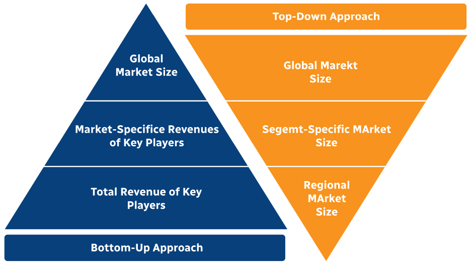
Methodology
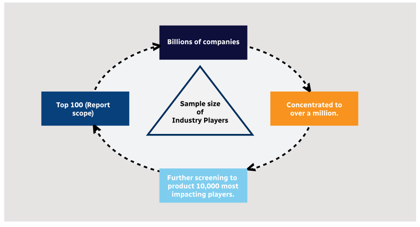
Step 1 - Identification of Relevant Samples Size from Population Database

Step 2 - Approaches for Defining Global Market Size (Value, Volume* & Price*)
Note*: In applicable scenarios
Step 3 - Data Sources
Primary Research
- Web Analytics
- Survey Reports
- Research Institute
- Latest Research Reports
- Opinion Leaders
Secondary Research
- Annual Reports
- White Paper
- Latest Press Release
- Industry Association
- Paid Database
- Investor Presentations

Step 4 - Data Triangulation
Involves using different sources of information in order to increase the validity of a study
These sources are likely to be stakeholders in a program - participants, other researchers, program staff, other community members, and so on.
Then we put all data in single framework & apply various statistical tools to find out the dynamic on the market.
During the analysis stage, feedback from the stakeholder groups would be compared to determine areas of agreement as well as areas of divergence